Part I The beginning
The processors we find today in our computers are beasts of power, not only because they have high frequencies, but also because they integrate advanced features that make executing instructions even faster, such as pipelines, caches, and threads (on x86_64).
Our smartphones are the same too, they are based on a System-on-Chip or SoC. They may not be as powerful as our desktop computers processors but they do provide a lot of features: SPI, I2C, DMA, I2S, LCD, etc...
Thus, what would be a good way to start getting familiar with embedded systems or hardware in general. Getting an MCU? Getting an SoC? A Raspberry Pi? An Arduino?
Why not make an 8-bit computer? We can still buy brand-new 8-bit processors like the Zilog Z80 or the 6502.. Even though they are not very powerful compared to what we are used to today, they are still very simple to set up, to use and to understand.
Why this Zeal 8-bit project
I started this project for several reasons. The first reason is that I have always wanted an 8-bit computer easy to use, easy to set up, able to play games on, write software on,and also easy to extend. Moreover, as I said above, making an 8-bit computer could help anyone who would like to understand more hardware and embedded systems.
Setting up a goal
Before starting making an actual 8-bit computer, I had to set up a goal. Here are the goals I set up upon starting:
- Simplicity: it should be simple to use and program for
- Programmable:
- Directly on it or from another computer then transfer to it
- In assembly and in a higher-level programming language (BASIC for example)
- With graphics, not only text
- With audio if time allows
- Hackable: it should
- Not be an emulation, so no MCU or SoC on it
- Be upgradable, so use sockets whenever possible
- Have one or more extension ports
I always kept these goals in mind as they will help (or constraint) me choosing some components more than others. In fact, some components are not available is DIP nor PLCC, no they cannot be socketed. In that case, I prefer to choose a similar part that exists in any of these packages.
Choosing the components
After setting the goals, I started checking for the exact parts that I wanted to use. Without hesitating, I chose the Z80 as a processor.
This processor from the late 70s was a huge success back then, it was used in the ZX Spectrum, TRS-80, Amstrad CPC and even the MSX standard. In fact, it is still manufactured today and we can still find in it some electronic devices, like scientific calculators for example. Interestingly, the Nintendo Gameboy and Nintendo Gameboy Color are based on a very similar processor.
Zilog Z80 and clock frequency
I decided to go with that version of the Z80, the one designed in the 70s and not the newer versions like the Z180 or eZ80. The second important point that needs to be decided is the processor frequency. The faster it is, the faster the instructions will be executed. However, this makes interfacing with the external components harder, as they would need to be fast enough to reply to the Z80 on time. The (CMOS) Z80 exists in several references, stating the maximum frequency it can operate on:
| Reference | Max. Frequency | Clock Cycle Time |
|---|---|---|
| Z84C0004 | 4MHz | 250ns |
| Z84C0006 | 6MHz | 166ns |
| Z84C0008 | 8MHz | 125ns |
| Z84C0010 | 10MHz | 100ns |
| Z84C0020 | 20MHz | 50ns |
Note: the maximum frequencies are the one given officially by Zilog, in practice, this may differ. In fact, from my experience, it is possible to make a Z84C0008 run at 10MHz, but it will draw more current and may heat more than when running at 8MHz.
The Z80 is rather slow in terms of instruction execution, in fact, the fastest instructions take 4 clock cycles to execute, this means that if we have 4MHz, in the best case, we will be able to execute 1 million instructions per second. Indeed, this Z80 has no pipeline and no cache.
After thinking about this, I made my choice, I will run everything at 10MHz!
ROM and RAM
Having a running processor is nice, but it is useless if we don't have code to execute, this is why we need a component which stores code to be executed by the processor. This component is a Read Only Memory or ROM. This is in fact a generic name, EPROM, EEPROM, NOR FLASH can also be considered as ROMs.
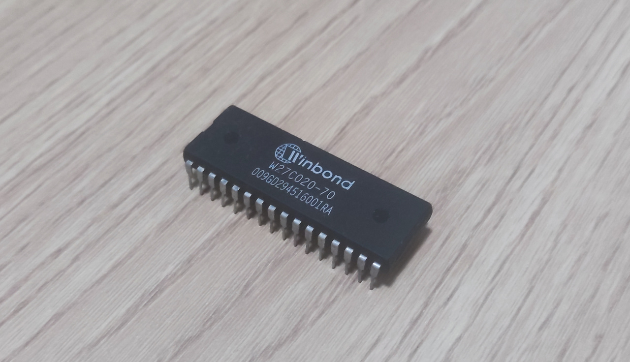
The one I started with is the Windbond W27C020-70. This chip is an EEPROM, which means that it can be erased electrically, without the need of UV light (as opposed to EROM), its size is 256KB, and it is more than enough for executing some fun software.
Regarding the RAM, or Random Access Memory, I decided to start with the AS6C1008, which stores 128KB. It is a Static RAM, or SRAM, so it doesn't need to be refreshed, as opposed to Dynamic RAM (or DRAM). It will store the stack and also all the variables required by the system and the programs.
Memory mapping
After choosing the components, the question was how to interface everything together? In fact, the Z80's address bus is 16-bit wide, so it can address up to 64KB, from 0x0000 to 0xFFFF. After booting, the Z80 starts executing the code at address 0, so we must have some code mapped there, and as the code is contained in the ROM, then the ROM will be mapped in the first part of memory.
The easiest way to separate the memory mapping is by splitting it in two: the first half is the ROM, the second half is the RAM, which gives us:
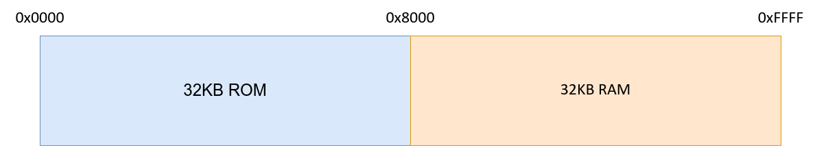
That would work great, but you may have guessed the issue that we are going to have: our ROM size is 256KB and the RAM size is 128KB, how can we fit that inside the memory mapping?
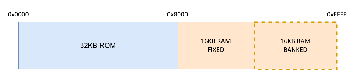
A solution to this is memory banking. It consists in switching, in the hardware, the part of the ROM or RAM that will be seen by the system, in software. In my case, I decided to split up the RAM part of the memory (32KB) in two. The first 16KB became the bankable memory, the second part was fixed. Diagrams will help here to understand. The memory mapping now looks like this:
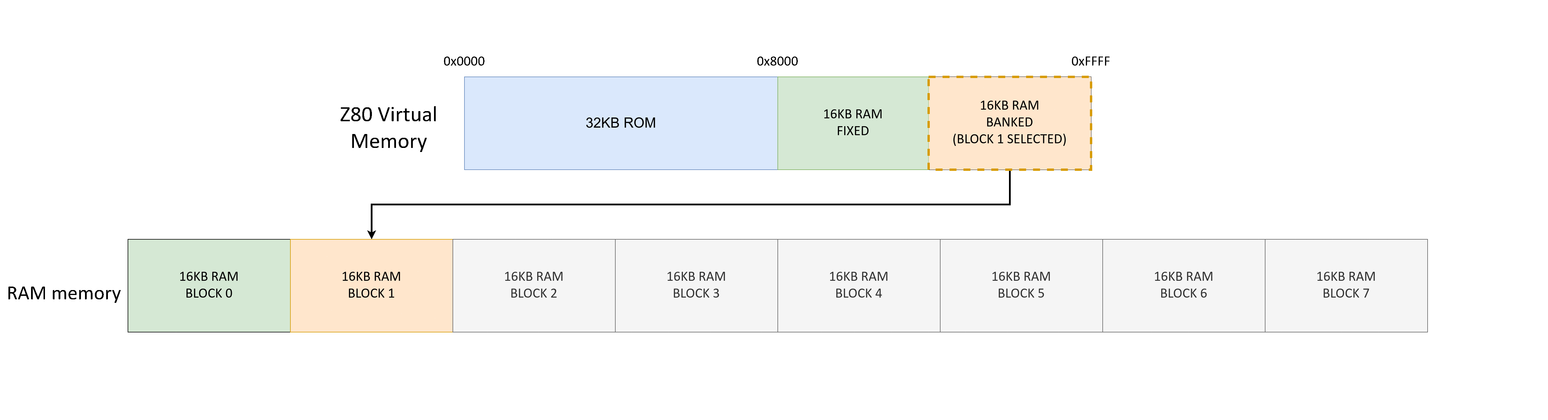
Now, I decided that the fixed part will be mapped to the first 16KB of the RAM, the banked one will be configured by the software to point to any of the 7 remaining 16KB RAM blocks (128KB/16KB = 8 but the first one is always in the fixed part). This looked like this:
I/O Bus
As you saw in the previous section, the memory mapping only presents ROM and RAM, but nothing regarding the I/O, not even a part of the memory for configuring the banked memory. In fact, the Z80 has a dedicated I/O bus, this is where we can/should place anything related to I/O. This bus is officially 8-bit, but in practice it can be used as 16-bit bus, just like the regular memory one. For the whole project, I will consider the I/O bus as an 8-bit bus, so the addresses go from 0x00 to 0xFF.
This is where we will map the banked memory configuration register.
In the software, in order to access the I/O bus, there are specific instructions, such as out, in, outi, ini, etc...
Apart from the fact that the memory and I/O bus are separated, the main difference is also the speed. Indeed, the Z80 will take more time to perform an I/O operation. Technically speaking, this is due to the fact that the Z80 deliberately inserts a WAIT signal on its line in order to give one more clock cycle to the external peripherals to perform and finish the I/O request.
I won't enter into details here as there will be a section dedicated to timings, but as a simple example, if our Z80 is running at 10MHz, reading memory address contained in HL with the instruction ld a,(hl) will take 0.7µs, whereas reading I/O port 0xFF with in a,(0xFF) will take 1.1µs.
Peripherals
After learning more about the I/O bus, I knew this was to place to put the memory banking configuration register. I needed to settle what this configuration register would be concrete. The RAM is 128KB, so the biggest address is 0x1FFFF, it has 17-bit, whereas the virtual memory page is 16KB (fixed part is also considered a memory page), so it has 14 bits. The problem is now obvious, there are 3 bits difference between the two addresses, so I needed a way to store and provide these bits to RAM. This is why I chose to use an 8-bit register as the memory banking register.
Out of the 8 bits, 3 would be used by the RAM, instead of disregarding the spare 5 bits, I decided to connect them to LEDs, this is a nice way to have feedback from the board.
In the next part
So far in this part, we have decided on the project goals, CPU frequency, RAM, ROM, memory mapping, and how we will configure everything. In the next part, it will be more practical, I'll explain how I came up with the first prototype.