Zilog Z80 Processor
6.1 Overview
The processor represents the computer's brain, it is the central piece of this orchestra. It provides and masters the address and data buses which are the main hardware routes that will contain the data that are shared across all the components present on the motherboard. It is responsible for initiating all the transactions that are composed of reading, executing, and writing from and to memory and I/Os.
6.2 Hardware implementation
On Zeal 8-bit Computer, the processor is a Zilog Z80 CPU Z84C0010VEG, referenced U2, and presented in a PLCC44 package. This package was chosen for its smaller form factor, compared to the traditional DIP32, while providing the same features and still supporting a clock frequency of 10MHz.
The pinout of the processor on the motherboard is as follows:
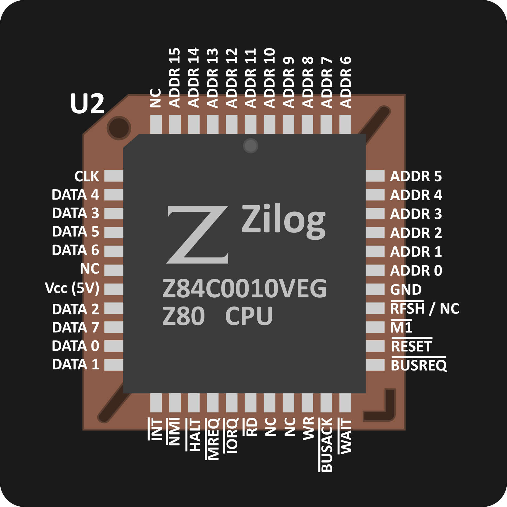
Where the pins represent:
- $CLK$: clock signal, coming from the active oscillator presented previously. On Zeal 8-bit Computer, it is a stable 10MHz clock signal.
- $ADDR\ 0$ to $ADDR\ 15$: represent the virtual address the CPU is trying to access, used for both the I/O and the memory bus.
- $DATA\ 0$ to $DATA\ 7$: bi-directional bus representing the byte to write to memory or I/O, or the byte read from memory or I/O.
- $\overline{RD}$: active (low) when the CPU is performing a read. In this case, the $DATA$ bus is put in high-impedance so that it can be driven by the component mapped at the address represented by $ADDR\ n$ lines.
- $\overline{WR}$: active (low) when the CPU is performing a write. In this case, the $DATA$ bus is driven by the CPU and contains the byte to write to the component mapped at the address represented by $ADDR\ n$ lines.
- $\overline{MREQ}$: active (low) when the CPU is performing a memory request operation. This is the case when memory instructions are used, e.g.
ld,ldi,ldir,cpi, etc... More information about the memory bus in the section Memory requests. - $\overline{IORQ}$: active (low) when the CPU is performing an I/O request operation. This is the case when I/O instructions are used, e.g.
in,ini,out,outi, etc... More information about the memory bus in the section I/O requests - $\overline{M1}$: active (low) when the CPU is currently fetching the next instruction to execute. This signal stays active during two T-states (clock cycles), during the second clock cycle, both $\overline{RD}$ and $\overline{MREQ}$ will be active. More information about this signal in the Instruction fetch section.
- $\overline{WAIT}$: input signal used to tell to CPU to insert one more clock cycle to the current read or write operation. This can be used when the device cannot reply on time to the read or write request made by the CPU. On Zeal 8-bit compute motherboard, it is not used for any device, but it is available on the extension port. As such it can be freely used by an external component. Moreover, this line is already pulled up with a 1kΩ resistor.
- $\overline{INT}$: open-drain input line to request a maskable interrupt to the CPU. It will only be taken into account if the interrupts are enabled in software by executing
eiinstruction. It is connected to the Z80 PIO, the I²C internal connector and the extension port. This line is pulled up with a 1kΩ resistor. More information about interrupts in the interrupts section below. - $\overline{NMI}$: input line to request a non-maskable interrupt to the CPU. This special interrupt has a higher priority than the ones requested with $\overline{INT}$ line. This line is pulled up with a 1kΩ resistor and is available on the extension port. More information about interrupts in the interrupts section below.
- $\overline{BUSREQ}$: input signal used to take the arbitration of both the address and the data buses. In other words, it tells the CPU to release all the address, bus, $\overline{WR}$, $\overline{RD}$, $\overline{MREQ}$ and $\overline{IORQ}$ lines by putting them into a high-impedance state. As such, another master can use these lines to communicate with the devices present on the computer. For example, this can be used for DMA chips. It is currently not used but is already pulled up with a 1kΩ resistor. It is available on the extension port.
- $\overline{BUSACK}$: active (low) after a device set $\overline{BUSREQ}$ to low when the CPU has put the memory control lines to high impedance. In other words, it is used by the CPU to tell the device that requested the bus that it can now use the buses freely. This line is connected to the MMU to make sure it is only enabled when the CPU is the bus master. More information about this in the MMU section.
- $\overline{HALT}$: active (low) when the CPU is halted after executing the
HALTcommand. It is currently not used but is available on the extension port. - $\overline{RFSH}$ / NC: Refresh signal generated after each instruction fetch, meant to be used to refresh dynamic RAM (DRAM). Since Zeal 8-bit Computer only uses SRAM, this signal is unused and not connected.
- Vcc and Gnd: 5V power supply.
The pins marked with a bar on top of them mean they are active low, i.e. they are considered active when the voltage across them is near 0V.
6.3 CPU speed and clock signal
The CPU speed depends on the number of instructions it can execute per second. The Z80 CPU used on Zeal 8-bit Computer is the Z84C0010 which is marked to support a clock up to 10MHz.
That 10MHz signal is coming from the active oscillator presented in the previous Clock circuit section. At each clock period, named T-State, the Z80 changes its internal state. It goes through several states, named Machine State, to execute an instruction, this is why it requires several clock cycles to execute a single instruction, even the simplest ones like nop!
Therefore, the number of instructions it can execute per second is much lower than the clock frequency. In the case of Zeal 8-bit Computer, it is around 1.45 million.
6.4 Boot up
On power up, the Z80 CPU requires the $\overline{RESET}$ signal to be active for a few clock cycles. As we saw in the Power-on and reset circuit section this is done thanks to a supervisory reset circuit, which holds the $\overline{RESET}$ line for more than 100ms.
After the $\overline{RESET}$ signal is de-asserted, the CPU will start executing the first instruction at address 0x0000. This means that on boot up, 0x0000 virtual address must point to a non-volatile memory, such as a ROM. On Zeal 8-bit Computer, this is the case, after a reset, the first 16KB of the ROM is mapped to virtual address 0x0000.
6.5 Memory requests
The official Z80 user manual is very rich in resources and technical details about how the processor timings and the requests it makes to the external components. This is why in the following sections, we will concentrate on the practical side of the timings and how it works on Zeal 8-bit Computer.
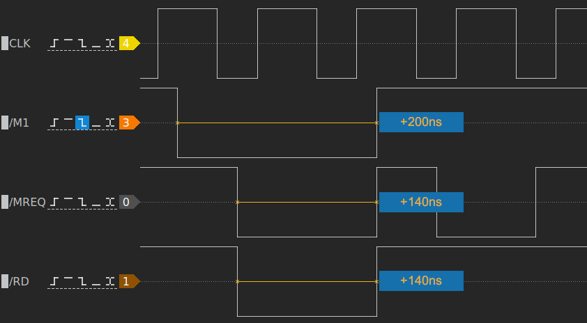
Instruction fetch
To execute an instruction from memory, the Z80 first needs to fetch it, to read it. To do so, it set its $\overline{M1}$ line to low while putting its Program Counter (PC) register on the address lines. Half a clock cycle later, both $\overline{MREQ}$ and $\overline{RD}$ go active. Since the address is already stable when these two lines go low, they can be used as Chip Enable and/or Output Enable for memory chips. These three lines are de-asserted 1.5 clock cycles later, while $\overline{RFSH}$ is activated.
Overall, the flow is as follows:
- $\overline{M1}$ is set to low, PC is set to address lines
- 0.5 clock cycle later, $\overline{MREQ}$ and $\overline{RD}$ go low
- 1.5 clock cycles later, all three lines are set to high, $\overline{RFSH}$ is set to low.
- 2 clock cycles later, $\overline{RFSH}$ is set to high.
Therefore, any instruction on the Z80 takes at least 4 clock cycles (T-States), which equals 400ns.
The following image shows the timings measured in practice:
Memory read and write
After the instruction is fetched by the Z80, it is executed. If the instruction is composed of more than a single byte, such as ldir, or if it has a parameter, such as ld a, 0x42, or it is a memory load, such as ld a, (hl), the processor will continue with another memory load.
Memory loads during execution are very similar to the fetch process, with the difference being that $\overline{M1}$ line is high and both $\overline{MREQ}$ and $\overline{RD}$ lasts 2 clock cycles instead of 1.5 when fetching.
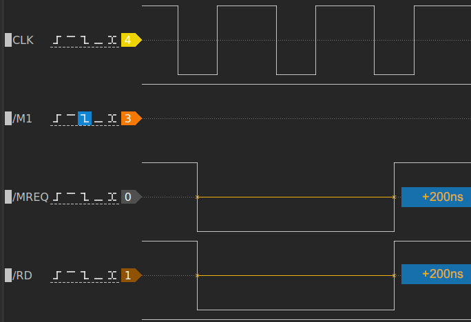
Again, the CPU here latches the value of the $DATA$ bus on the rising edge of these two lines.
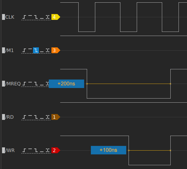
For memory writes, the process is different: the $\overline{MREQ}$ goes low first, to signal that the byte to write to memory is ready on the $DATA$ bus. Then, 1 clock cycle later, $\overline{WR}$ line goes low. It remains low for a single clock cycle. Of course, during the whole process, $\overline{M1}$ and $\overline{RD}$ are always high.
Memory WAIT cycle
As we just saw, on Zeal 8-bit Computer a memory read takes around 200ns to be performed, while a memory write takes 100ns. This means that the device that needs to be read from or written to needs to be fast enough in both cases to be interfaced with the Z80.
If the device is not capable of replying to the request within this delay, it is possible to tell the Z80 to wait longer. This is done thanks to the $\overline{WAIT}$ signal, it must be active (low) as long as the device needs.
It is not used on Zeal 8-bit Computer since all the devices are compliant with the 10MHz clock requirement, but the signal is still usable and present on the extension port.
6.6 I/O requests
During memory requests, the $\overline{MREQ}$ line was set to low by the processor to show that all the 16-bit on the address bus were ready to be read by the devices.
The Z80 has a second bus, namely I/O Bus, which is officially an 8-bit bus. It allows at most 256 different addresses from 0x00 to 0xFF. This secondary bus lets Z80-based computers only have RAM and/or ROM in their main address space and have the slower devices, responsible for the I/Os, in this secondary address space. As such, there is no need for memory-mapped I/Os, which usually makes the memory mapping more complex and wastes bytes that cannot by used by memory devices.
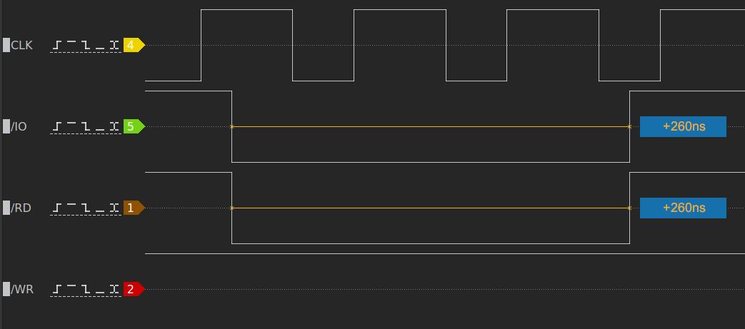
During read I/O requests, the CPU outputs the address on the first clock cycle, on the second clock cycle it activates $\overline{IORQ}$ and $\overline{RD}$ lines. This time, the CPU internally inserts a single WAIT. As such, these two lines keep low for 2.5 clock cycles:
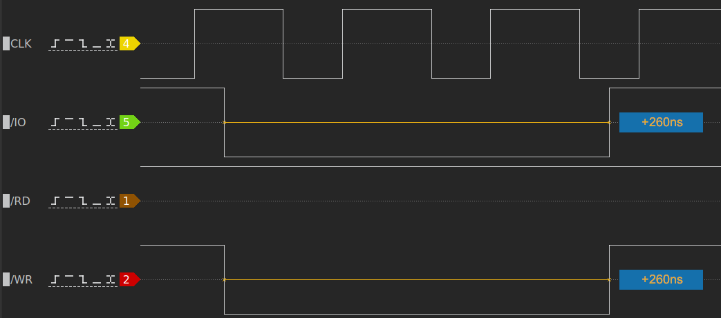
The process is the same for write I/O requests, but the CPU asserts the $\overline{WR}$ line instead of the $\overline{RD}$ line:
A small note regarding I/O requests and the address lines. Even though Zilog claims that the I/O bus is an 8-bit bus, when the software executes an I/O request, the upper 8 bits of the address bus are deterministic and documented:
- When
nis used as the I/O address, the 16-bit address lines are set toAregister for the upper 8-bit part andnfor the lower part. - When
Cis used as the I/O address, the 16-bit address lines are set toBregister for the upper 8-bit part andCfor the lower part.
For example, if the software is as follows:
ld bc, 0x1267
in a, (c)
The 16-bit address put on the address lines during the IO request is 0x1267.
If the software is as follows:
ld a, 0x42
in a, (0x98)
The 16-bit address put on the address lines during the IO request is 0x4298.
6.7 Interrupts
As Zeal 8-bit Computer doesn't make use of the non-maskable interrupt line $\overline{NMI}$ but uses the maskable interrupt line $\overline{INT}$, we will only tackle the latter. Keep in mind that the $\overline{NMI}$ is documented in the official Z80 user manual and that this pin is available on the extension port, it can therefore be used by external boards.
On the motherboard, the $\overline{INT}$ line is connected to both the Z80 PIO and the internal I²C internal connector. When that line is activated by any requesting device, the Z80 CPU samples it at the end of the current instruction. As soon as it acknowledges the $\overline{INT}$ line, it will set $\overline{M1}$ line to low, then, 2.5 clock cycles later, it sets $\overline{IORQ}$ line to low. From that point, both will stay low for around 1.5 clock cycles, and the data bus is put in high impedance.
In total, when the Z80 acknowledges an interrupt, the $\overline{M1}$ line is kept low for 4 clock cycles, which is around 400ns, and $\overline{IORQ}$ is kept low for around 1.5 clock cycles, or 150ns. During that moment, the CPU may be waiting for a byte to be received from the device that initiated the interrupt. This behavior depends on the Interrupt Mode it has been configured to use in software with the instruction im x, where x is 0, 1 or 2.
📝 Note
The CPU only accepts these interrupts if the software has enabled them beforehand with the instruction
ei. Moreover, interrupts are disabled on boot, which means it is mandatory to useeiat least once to start receiving interrupts.
Mode 0
This mode can be selected by executing the instruction im 0. In this mode, during the clock cycles where the $\overline{IORQ}$ line is low, the device that requested an interrupt must place a byte on the data bus that will be executed by the CPU. In other words, the requesting device has to give the CPU an instruction.
This mode is not used on Zeal 8-bit Computer by default.
Mode 1
This mode can be selected by executing the instruction im 1. In this mode, the CPU isn't expecting any byte during the clock cycles where the $\overline{IORQ}$ line is low. Indeed, the content of the DATA bus will be ignored and the CPU will execute a restart at virtual address 0x0038. In other, it will save the current Program Counter on the stack and set it to 0x0038, which is the equivalent of a call 0x0038.
This mode is not used on Zeal 8-bit Computer by default.
Mode 2
This mode can be selected by executing the instruction im 2. In this mode, during the clock cycles where the $\overline{IORQ}$ line is low, the device that requested an interrupt must place a byte on the data bus that represents the index of an address in the vector table whose address upper byte is stored in I register. Then, the CPU reads that address from memory and jumps to where it points.
Therefore, the I register must be set before enabling the interrupts. Here is an example to understand how it works, let's say we have the following snippet of code:
    ; This routine is the first one that will be executed in our example
_start:
    ; Set the I register to the vector table address defined below. I shall contain the high byte only
    ld a, my_vector_table >> 8
    ld i, a
    ; Switch to interrupt mode 2 and enable interrupts
    im 2
    ei
    ; Wait for an interrupt
wfi:
    halt
    jp wfi

    ; It is advised to have my_vector_table aligned on 256 so that its lowest byte is 0
my_vector_table:
    DEFW handler_1
    DEFW handler_2
    ; ....
    DEFW handler_256

    ; Interrupt handler for one device
handler_1:
    ; Do something...
    ; Re-enable interrupts and return from interrupt
    ei
    reti

    ; Interrupt handler for another device
handler_2:
    ; Do something...
    ; Re-enable interrupts and return from interrupt
    ei
    reti
Let's suppose we have device A configured to send the bytes 0x02 when requesting an interrupt to the Z80 CPU. The flow of interrupting the CPU is as follows:
- The device
Adrives $\overline{INT}$ line low to request an interrupt to the CPU. The device now waits. - The CPU sets $\overline{M1}$ line low first and then sets $\overline{IORQ}$ line low afterward, waiting for the device (
A) to send a byte. - The device notices that both $\overline{M1}$ and $\overline{IORQ}$ lines are low, it outputs pre-configured byte
0x02on the DATA bus. - The CPU rises both lines high while sampling the byte,
0x02, from the DATA bus. It will also push the current Program Counter on the stack. - The CPU forms a 16-bit address by concatenating this new byte to the
Iregister, so we getVECT_ADDR = (I << 8) | 0x02. - The CPU reads two bytes from the memory address
VECT_ADDR, it finds routinehandler_2address, which is the second entry in themy_vector_tablearray. (the equivalent notation in C would be*(my_vector_table + 2) = handler_2) - The CPU disables interrupts and jumps to
handler_2routine.
📝 Note
It is not mandatory to have 256 entries in the vector table, if only a single device is used for interrupts or if the pre-configured index values are known, it is possible to have a very small vector table.
Similarly, it is not strictly necessary to have the vector table to be aligned on 256, but it would mean that the low byte of its address would need to be part of the index to configure to the interrupting devices. However, for simplicity reasons, it is advised to have a vector table aligned on 256. (lowest byte of the its address equal to
0x00)