Read-only Memory (ROM)
9.1 Overview
As we saw earlier, after the CPU starts or resets, it will start executing code from the first virtual address: 0x0000, which is also equal to 0x000000 physical address at this stage.
As such, this address must also present some valid binary code that the CPU can understand and execute, so we need a device to store this data. This is where the Read-Only Memory, or ROM, comes in: it will store the code the CPU will execute.
9.2 Hardware implementation
Despite its name, the Read-Only Memory, or ROM, is not necessarily non-erasable, it exists several types of ROM that can be erased and re-written: EPROMs, EEPROMs, NOR Flash, NAND Flashes, ...
On Zeal 8-bit Computer, the component that acts as a ROM is the SST39SF020 NOR Flash of 256KB, organized as 256K words of 8 bits, and referenced U4 on the PCB. It is presented in a PLCC32 package in a socket, making it compact but still with the possibility to remove it and re-insert it easily, without the need to solder or desolder anything.
The main advantages of this SST39SF020 NOR Flash are:
- Programmable in-circuit, no need to take it out and use a special programmer to erase or re-write it, this can be done directly from the Z80!
- Doesn't require any special hardware protocol to be erased or programmed, it still acts as a regular (EEP)ROM from the CPU point of view.
- Big capacities for an 8-bit computer: up to 512KB.
- Pin-to-pin compatible with the legacy 27C020 ROM.
- Availability, they are easy to find as they are still manufactured in big quantities.
In terms of pinout, here is how it is organized:
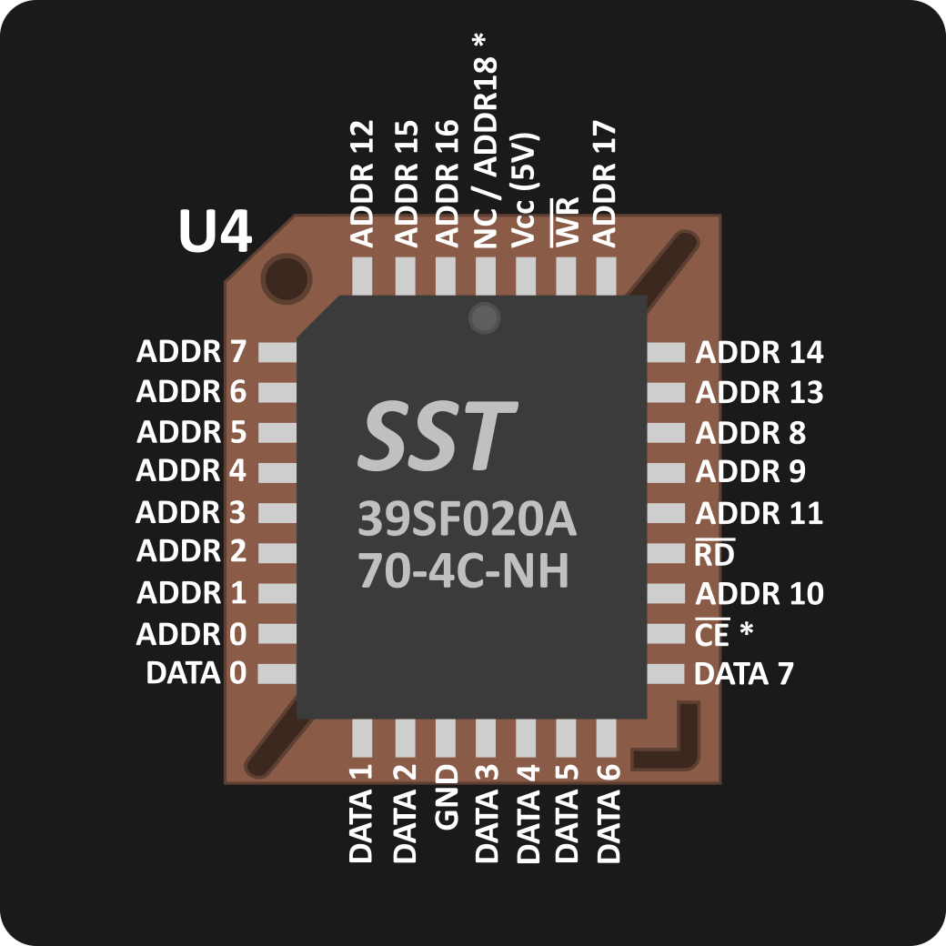
Let's see the regular signals connected to it:
- $ADDR\ 0$ to $ADDR\ 17$: represent the address of the byte to read from. The ROM is 256KB, so the last byte address is
0x3ffff. - $DATA\ 0$ to $DATA\ 7$: represent the byte that was just read from the ROM.
- $\overline{RD}$: signal coming from the CPU, active when the CPU is performing a read.
- $\overline{WR}$: signal coming from the CPU, active when the CPU is performing a write. More info in the programming the ROM section.
- $\overline{CE}$: signal coming from the logic glue, active when the CPU tries to access the address range where the ROM is mapped, which is the first 512KB of the physical address space. More info in logic glue chapter.
Two signals, marked with an asterisk, present a special feature or state, the sections below explain these details.
9.3 Hardware dependencies and timing
In terms of timing, the ROM depends on the MMU, as it requires the 18 or 19 address lines, depending on the size of the ROM, but also on the logic glue. Indeed, the latter outputs the $\overline{ROM\_ENABLE}$ which is connected to the ROM's $\overline{CE}$ signal. Both should be taken into account to determine the ROM's total propagation delay between the moment the CPU performs a read and the ROM outputs the data.
According to the datasheet, the SST39SF020A-70 itself is marked as having a propagation delay of 70ns in the worst case.
All the details about the delay and timings are explained in the official datasheet.
9.4 Installing a bigger NOR Flash
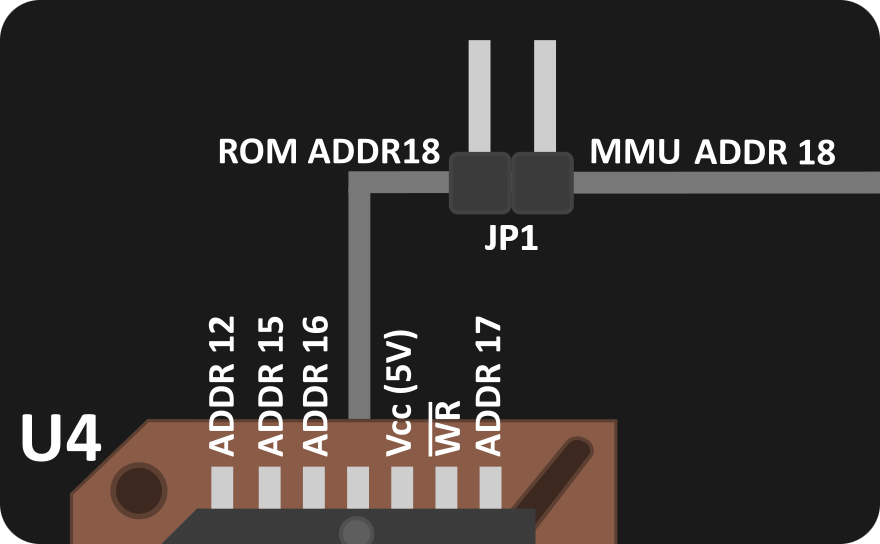
The first pin of the ROM, $NC / ADDR\ 18$, has two possible states: in the case where a 256KB ROM is installed in the socket U4, which is the default case, this pin must be left unconnected.
However, if a 512KB ROM is installed instead, like the SST39SF040 for example, this pin must be connected to $ADDR\ 18$ coming from the MMU. To do so, it is simply required to connect a jumper on the bridge referenced JP1 on the PCB.
By connecting this bridge, the $ADDR\ 18$ of the MMU will be connected to this pin, giving the Z80 CPU access to the whole 512KB of ROM available.
This jumper, JP1, explains why we needed to allocate 512KB of contiguous memory to the ROM in the logic glue. If only 256KB were allocated (from 0x00000 to 0x3ffff), replacing the ROM with a 512KB one would be more difficult since it would require additional logic to map the second 256KB part of the ROM.
Schematically, it looks as follows:
9.5 Disabling the ROM
As described in the logic glue chapter, no matter if the installed ROM is 256KB or 512KB big, the ROM's $\overline{CE}$ signal will be active whenever the CPU tries to read (or write) to any physical address between 0x00000 and 0x3ffff.
One consequence of this is that the ROM is always the first place where the CPU will get its instructions from. However, in some cases, it is interesting to have an external bootable cartridge that will completely bypass Zeal 8-bit Computer's internal ROM and only lets the CPU read and execute data from the ROM embedded in that new external board.
One solution would be to simply remove the internal ROM momentarily, and plug the extension board, as such, there will be no conflict between the ROMs. The other solution which involves no motherboard modification is to pull $\overline{CE}$ line high, making it non-active.
To do so, signal $\overline{CE}$ is connected to the logic glue's $\overline{ROM\_ENABLE}$ signal through a 1kΩ resistor (referenced R5) and is also connected to the extension port (referenced J2) pin 49 without any resistor.
As such, whenever the external extension board needs to disable the internal ROM, this ROM_DISABLE pin must be set to high (5V). Check the extension port section to see its exact position.
9.6 Programming the ROM
NOR Flash, just like EPROMs and EEPROMs can be programmed thanks to some universal programmers.
However, as stated previously, the main advantage of a NOR Flash, over the previously cited ROMs, is that it can be programmed in-circuit, without taking it out of its socket and so, without the need for such universal programmers.
The whole process of erasing and programming the NOR flash is explained in the official datasheet.
Programming theory
In short, the NOR flash realizes this thanks to software commands that are composed of successive writes at pre-defined addresses with pre-defined values, as described in this table taken from the document linked above:
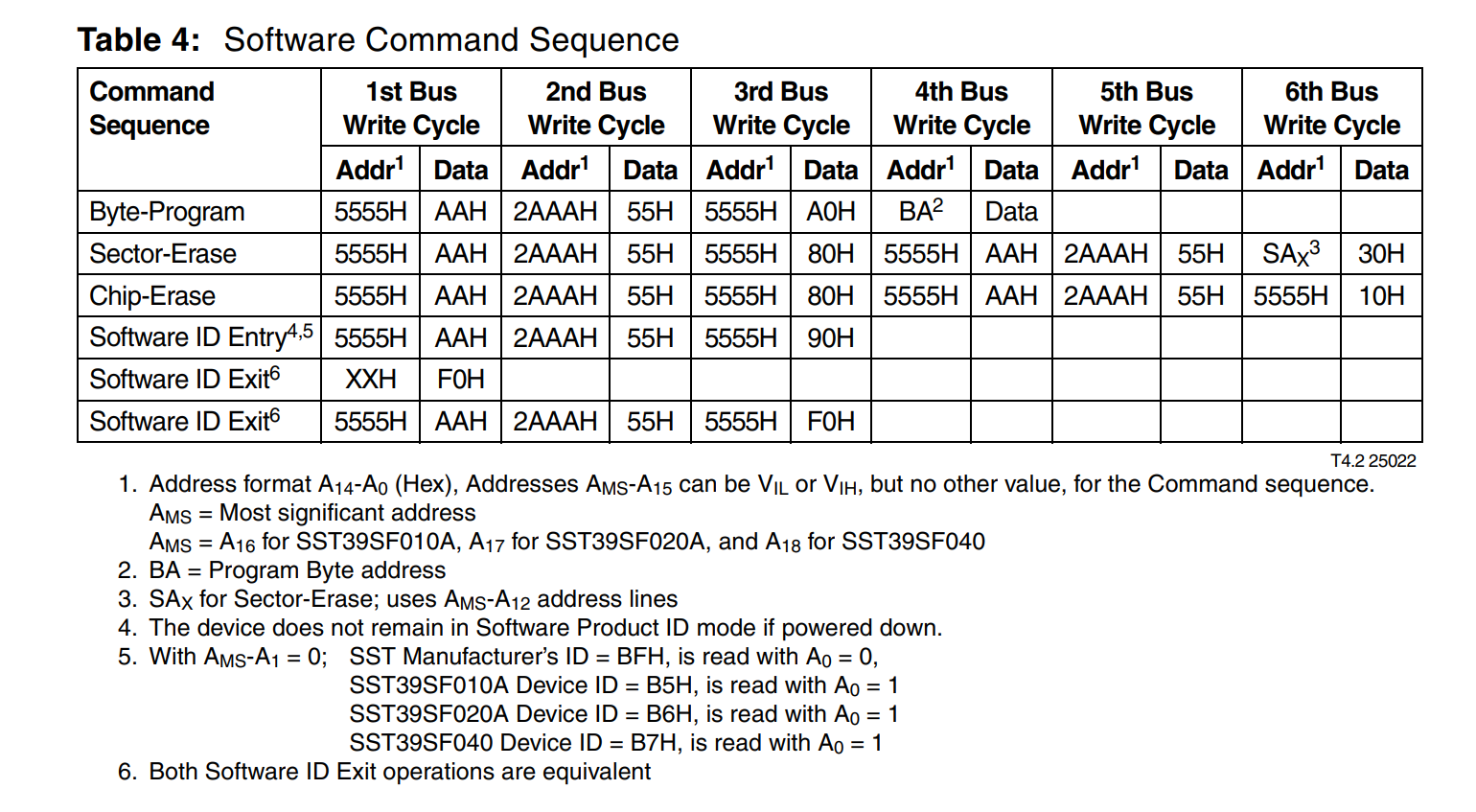
It is important to note that these addresses are addresses relative to the NOR Flash, but as the NOR Flash is mapped at physical address 0x00000 on Zeal 8-bit Computer, we can consider them physical addresses, and not virtual addresses!
In other words, to perform any of these commands, at least two 16KB pages of the ROM must be mapped into the 64KB virtual address space. These two pages are the ones containing bytes at address 0x2AAA (page 0) and 0x5555 (page 1) respectively. They may not necessarily be mapped at the same time.
Another important thing to note is that in it is necessary to first perform an erase before attempting to program a byte. As such, even if a single byte of a sector must be (re)programmed, the whole sector must be erased first!
Practical example
As described in the previous table, the steps to erase the chip are:
- Write
0xAAto ROM address0x5555 - Write
0x55to ROM address0x2AAA - Write
0x80to ROM address0x5555 - Write
0xAAto ROM address0x5555 - Write
0x55to ROM address0x2AAA - Write
0x10to ROM address0x5555
Then the NOR Flash will start erasing itself, this will take at most 100ms. This means that the program that erases the Flash must not be in the Flash itself, else it will get erased, it should be executed from another place, like RAM.
Here is a practical example, in Z80 assembly, of how to erase the chip with a software command:
    ; The following code is run from RAM, at virtual address 0x8000
    ; First two 16KB virtual pages are free, we can use them to map ROM's first pages
erase_chip:
    ; Initialize A to 0
    xor a
    ; Map virtual page 0 to physical addresses 0x0000 - 0x3FFF
    out (0xF0), a
    inc a
    ; Map virtual page 1 to physical addresses 0x4000 - 0x7FFF
    out (0xF1), a

    ; We now have access to NOR flash addresses 0x2AAA and 0x5555, start the erase process
    ld hl, 0x5555
    ld a, 0x55
    ; 1. Write `0xAA` to ROM address `0x5555`
    ld (hl), 0xAA
    ; 2. Write `0x55` to ROM address `0x2AAA`
    ld (0x2AAA), a
    ; 3. Write `0x80` to ROM address `0x5555`
    ld (hl), 0x80
    ; 4. Write `0xAA` to ROM address `0x5555`
    ld (hl), 0xAA
    ; 5. Write `0x55` to ROM address `0x2AAA`
    ld (0x2AAA), a
    ; 6. Write `0x10` to ROM address `0x5555`
    ld (hl), 0x10

    ; Wait for at least 100 ms for erase completion = 1,000,000 T-states at 10MHz
    ; 24 is the number of T-states below
    ld bc, 1000000 / 24
wait:
    ; 24 T-states for the following, until 'jp nz, _zos_waste_time'
    dec bc
    ld a, b
    or c
    jp nz, wait

    ; 100ms elapsed, chip is erased.