Video card connector
19.1 Overview
With all the components we saw up to now, we can qualify the motherboard as a standalone computer. Inputs can happen thanks to the PS/2 interface, the UART and the GPIOs, whereas the output can be realized through the UART with a serial monitor or a custom extension board. For custom boards that generate a video signal, another port than the extension port is available.
19.2 Hardware implementation
To be future-proof and to offer more versatility a video card connector, or video port, can be found on the motherboard. It is referenced J6 and is made out of a 2x20 2.54mm pin footprint, which makes it compatible with several types of standard connectors available on the market.
The main difference between this connector and the extension port is its location. Located on the right side of the board, it is designed to accommodate an extension board that can potentially sit in the same case as the motherboard. Moreover, that board would be responsible for the video signal generation, as such, it shall generate an H-Blank and V-Blank signals to the motherboard.
The pinout of the video card connector footprint from the top is as followed:
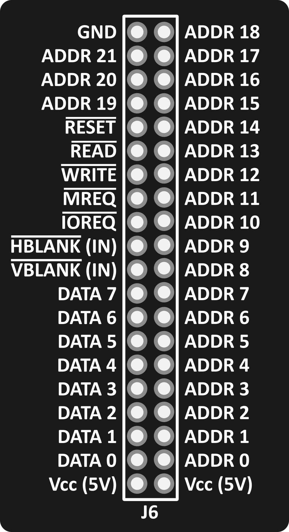
The signals are:
- $5V$ and $Gnd$: power output. The current drawn by the video board must not exceed 1A, else the fuse
F1will blow. - $A_0$ to $A_{21}$: address bus, corresponding to the current byte being accessed (read or written) on the 4MB physical address space by the CPU. The lines $A_0$ to $A_{13}$ are coming from the Z80 CPU directly, whereas the lines $A_{14}$ to $A_{21}$ are routed from the MMU.
- $D_0$ to $D_7$: data bus shared with all the other components. The video board must only output data on these lines if a request is performed to it, else these lines must be left in a high-impedance state by the video board.
- $\overline{HBLANK}$: input signal active when the screen is in H-Blank state, it shall be generated by the video board. This signal can be connected to the Z80 PIO and configured to trigger an interrupt in software.
- $\overline{VBLANK}$: input signal active when the screen is in V-Blank state, it shall be generated by the video board. This signal can be connected to the Z80 PIO and configured to trigger an interrupt in software.
- $\overline{RESET}$: reset signal coming from the Reset circuit, active on boot up or when the reset button, referenced
SW2, is manually pressed. - $\overline{WR}$, $\overline{RD}$, $\overline{IOREQ}$, $\overline{MREQ}$: signals that are coming from the Z80 CPU. They can be used to determine if a memory or an I/O operation is currently being performed. All the details about them can be found in the Z80 CPU section.
19.3 H-Blank and V-Blank signals
Horizontal blank, or H-blank, and vertical blank, or V-blank, signals shall be generated by the external video board. These signals can either be left unconnected to the rest of the motherboard or be connected to the Z80 PIO system port. To switch between these two features, the jumpers JP4 and JP3 can be set independently.
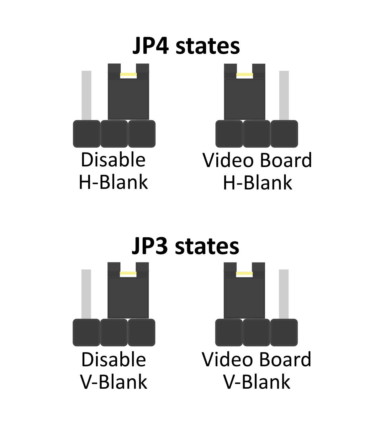
These states are also marked on the bottom silkscreen of the motherboard.
When the jumpers are wired to allow the H-blank and V-blank to be connected to the motherboard, these signals will first go through an open-drain buffer (74LS07), referenced U15 on the PCB. Thanks to this, it is safe to have 3.3V logic for both of them.
Here is a diagram that sums up how the signals are connected to the system.
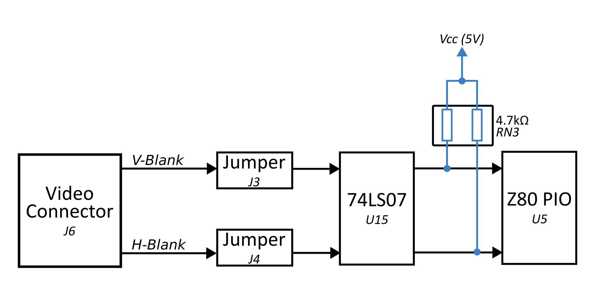
As both signals will end up on two different pins of the Z80 PIO, it is possible to configure them independently and enable an interrupt in the software.
19.4 Video board memory mapping
The connector doesn't provide any chip-enable signal that can be connected directly to the video board, instead, it provides all the physical address lines as well as the memory/io signals from the CPU. Thanks to this, the video board can be mapped anywhere on the 4MB except the first MB.
Indeed, the first 512KB are reserved for the ROM whereas the next 512KB is reserved for the RAM. The rest is free and can accommodate the VRAM and/or all the video registers.
Similarly, on the I/O bus, the addresses from 0x00 to 0x7f (included) are reserved for the users' extension boards, but addresses from 0x80 to 0xcf can be freely used by the video board.
You can refer to the memory mapping section for more information.
19.5 DMA capabilities
No component on Zeal 8-bit Computer motherboard uses Direct-Memory Access, or DMA, but the Z80 CPU does support it. While it is not always critical for regular memory transfers, for video memory it may be necessary.
The video connector presented above lacks the pins that are required to perform DMA. To keep the connector unchanged but still provide the possibility of having DMA for the external video board, another port is available: the DMA video connector. This port, referenced J7 on the PCB, is composed of 2 standard 2.54mm pins.
It is currently not populated on any Zeal 8-bit Computer motherboard. Here is a top-view of the connector:

Both $\overline{BUSRQ}$ and $\overline{BUSACK}$ come from the Z80 CPU directly. The first one is internally pulled up by a 1kΩ, so it doesn't need to be pulled on by the video board.
For more information about these signals, please refer to the Z80 CPU section.
As noted in the MMU section, when $\overline{BUSACK}$ goes low, meaning that the CPU releases all the request signals as well as data and address buses, the address lines from $A_{14}$ to $A_{21}$ will also be put in high-impedance state. The main consequence is that the video board must drive all the signals, including the 22 physical address lines, which can therefore be seen as a 4MB contiguous address space. The MMU cannot be used during a DMA operation and so, virtual pages cannot be managed.