Parallel I/O: Zilog Z80 PIO
11.1 Overview
Having a computer that runs complex programs is nice, but without any interaction with the outside world, it is useless. Its main purpose is to interact with the user, this is why we need some inputs and outputs or I/O.
The I/Os lets the CPU communicates with the outside world by toggling a pin, generating a signal that can be interpreted by any external entity or by reading a pin that is driven by such entities. As such, we can connect a mouse, a keyboard, a display, a storage device, etc...
11.2 Hardware implementation
On Zeal 8-bit Computer, the official Zilog Z80 PIO integrated circuit is used to provide GPIOs. Referenced U5 on the PCB, it is presented in a PLCC44 package, with a socket. It connects itself to the main data bus as it uses a parallel interface.
As it also requires the CPU clock line to be connected, the 10MHz variant of the Z80 PIO was chosen, the Z84C2010.
The main advantages of the Z80 PIO integrated circuit for our use cases are:
- Presents 2 ports, A and B, of 8 lines each
- Bit manipulation mode: lets us treat each line of a port independently from each other
- Fully compatible with Z80 CPU Mode 2 interrupt mode
- Well-documented and simple to program
- Uses parallel interface, connecting itself to the data bus
In terms of pinout, here is how it is organized:
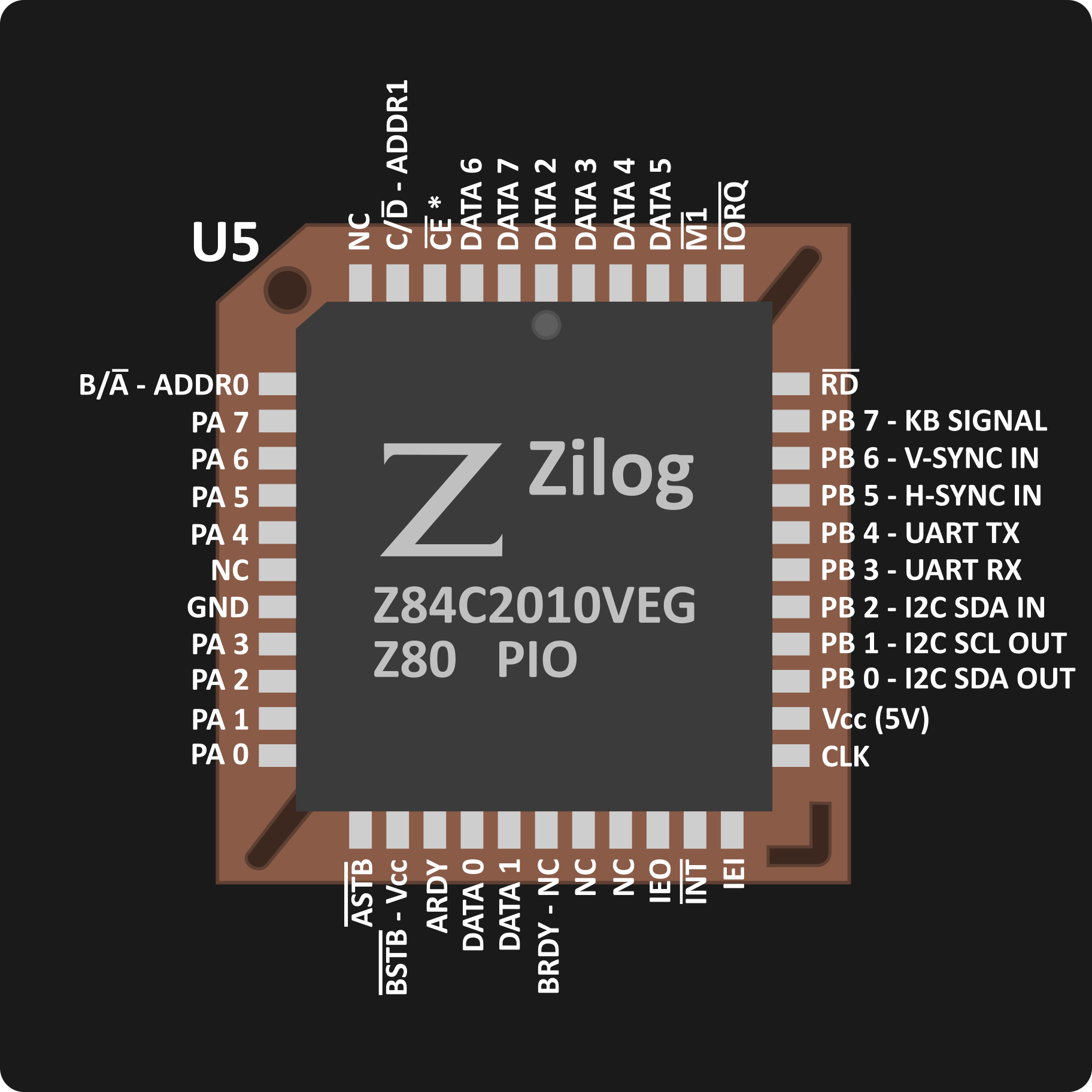
Some of the signals on the diagram above present two names separated by a dash -. The first description is the official name taken from the Z80 PIO datasheet, while the second one is the effective functionality given to that pin on Zeal 8-bit Computer motherboard.
Signals marked $NC$ are not connected to anything and must not be connected to any signal.
Here is a description of the pins responsible for ensuring the chip functions correctly:
- $DATA\ 0$ to $DATA\ 7$: data bus, common to all parallel components. Contain the byte to write to a particular I/O port or the byte read from a port.
- $\overline{CLK}$: signal coming from the 10MHz active oscillator, same clock that goes to the Z80 CPU.
- $\overline{RD}$: signal coming from the CPU, active when the CPU is performing a read.
- $\overline{IORQ}$: signal coming from the CPU, active when the CPU is performing an I/O request. As the PIO is mapped on the I/O bus, this signal must be active to enable the PIO.
- $\overline{INT}$: output signal used to request an interrupt to the CPU, note that this is an open-drain signal. In other words, the PIO only pulls it down when required, but never pulls it high, a 1kΩ pull-up resistor is responsible for this.
- $IEI$ and $EIO$: Interrupt input and output signals implemented by Zilog components to create a Daisy chain of interrupt with priority. These signals are not used in our case but are available through the extension port so that any Zilog component can be chained there. Note that $IEI$ is pulled up with a 1kΩ resistor.
- $\overline{M1}$: signal coming from the CPU, active when the CPU is performing an instruction fetch, mainly signal used to notify the PIO that the CPU is handling an interrupt.
- $\overline{CE}$: signal coming from the logic glue, connected to the $\overline{PIO\_ENABLE}$ signal, active when the CPU performs an I/O request to the PIO, which is mapped between [
0xD0,0xDF]. More info in logic glue chapter. - $B/\overline{A}$ - $ADDR\ 0$: signal used by the PIO to differentiate which port the CPU is trying to communicate with. When this line is low, port A is the recipient, when it is high, B is the recipient. On Zeal 8-bit Computer, this line is connected to $ADDR\ 0$.
- $C/\overline{D}$ - $ADDR\ 1$: signal used by the PIO to differentiate which registers the CPU is trying to read or write. When this line is low, the CPU reads or writes the current state of a port (I/O values). When it is high, the CPU reads or writes the configuration of one of the ports.
These latter three signals define the following I/O mapping for the PIO:
0xD0 - Port A Data
0xD1 - Port B Data
0xD2 - Port A Configuration
0xD3 - Port B Configuration

0xD4 - Same as 0xD0 (not recommended for use)
0xD5 - Same as 0xD1 (not recommended for use)
0xD6 - Same as 0xD2 (not recommended for use)
0xD7 - Same as 0xD3 (not recommended for use)

0xD8 - Same as 0xD0 (not recommended for use)
0xD9 - Same as 0xD1 (not recommended for use)
0xDA - Same as 0xD2 (not recommended for use)
0xDB - Same as 0xD3 (not recommended for use)

0xDC - Same as 0xD0 (not recommended for use)
0xDD - Same as 0xD1 (not recommended for use)
0xDE - Same as 0xD2 (not recommended for use)
0xDF - Same as 0xD3 (not recommended for use)
11.3 Ports A and B
The other pins present in the previous diagram are related to both ports A and B. The PIO can operate each port in four modes:
- Output: all 8 pins represent a single 8-bit output value
- Input: all 8 pins represent a single 8-bit input value
- Bidirectional: all 8 pins represent an 8-bit value that operates in both input and output.
- Bit Control: each pin is independent from the others, and thus can be independently input or output.
Since the bidirectional mode is only available on port A and forces port B to be in bit control mode, port A is considered the user port, freely usable by the user, and port B is the system port.
As such, the user has a total of 8 I/Os that can be freely used. More details are in the sections below.
11.4 User port
In the pinout shown above, the signals related to the user port, which is port A, are:
- ${PA}\ 0$ to $PA\ 7$: represent the 8 I/Os available on port A. They can be freely used by the user.
- $ARDY$: "ready" output pin used in different ways depending on the mode configured for port A:
- In output mode, it is active to indicate that the port was loaded with a new value that can be read.
- In input mode, it is active to notify the user that the port is empty and ready to receive data.
- In bidirectional mode, it is active to indicate that data is available on the port. However, the data will only be available on data bus if $\overline{ASTB}$ is active.
- In bit control mode, it is not used and is forced by the PIO to low.
- $\overline{ASTB}$: "strobe" input pin used in different ways depending on the mode configured for port A:
- In output mode, a positive edge issued by the peripheral tells the PIO the data written to the port were received successfully.
- In input mode, a strobe on the line stores the current data lines state in the PIO port A's internal register.
- In bidirectional mode, when the signal is active, port A's internal register value is placed on the data lines. A positive edge on this signal marks the receipt of the data.
- In bit control mode, it is not used/routed internally.
For further details about how the pins work, please check the official Z80 PIO user manual.
⚠️ Warning
Using bidirectional mode for port A requires both $BRDY$ and $\overline{BSTB}$ signal to be usable and available. However, as shown in the pinout above, $BRDY$ is not routed to external connector and $\overline{BSTB}$ is directly connected to $Vcc$ (5V). As such, using these pin would require to perform some hardware modification on the motherboard to have access to them.
It is however possible to simulate a simpler bidirectional port A by switching between input and output at runtime, in the software.
11.5 System port
Port B is used internally by Zeal 8-bit Computer, it must always be programmed in bit control mode as all the signals shall be managed independently:
- PB 7 - $\overline{KB\ Signal}$: input signal generated by the PS/2 keyboard circuit, goes low whenever a new byte from the PS/2 interface has been received. More details about it are in the PS/2 Keyboard section.
- PB 6 - $\overline{V Sync}$: input signal active when an external video card enters V-blank state. The original signal is located on the video connector, then it goes to an open-collector buffer, offered by the 74LS07 chip referenced
U15on the board, before entering the PIO through this pin. Thanks to this 74LS07 integrated circuit, the signal is open-drain and is pulled up by a 1kΩ resistor, referencedRN3. This also means that the original signal, coming from the video connector will be considered high if it has a voltage of at least 2V, as such, it is fully compatible with 3.3V logic levels. - PB 5 - $\overline{H Sync}$: input signal active when an external video card enters H-blank state. Same as the $\overline{V Sync}$ signal, it originates from the video connector, then goes through the 74LS07 buffer. It is also compatible with 3.3V logic levels. Both signals can be used for timing calculation since they occur at regular intervals.
- PB 4 - UART TX: output signal connected to the user port via a 512Ω resistor. As its name states, its goal is to be used as a UART Transmit (TX) signal, however, as Zeal 8-bit Computer doesn't present any UART or Serial chip, this signal must be simulated in software.
- PB 3 - UART RX: output signal connected to the user port via a 512Ω resistor. As its name states, its goal is to be used as a UART Receive (RX) signal. Again, this signal must be simulated in software for the same reason. More details will be given in the UART section.
- PB2 - I2C SDA IN: input signal connected to I2C devices described in Inter-Integrated Circuit (I²C) section also well as user port. Used to read the current status of SDA line, this is an open-drain signal that goes through the same 74LS07 chip. For the same reason as the UART, this signal is simulated in software.
- PB1 - I2C SCL OUT: output signal connected to I2C devices described in Inter-Integrated Circuit (I²C) section also well as user port. Used to output a clock signal used simulated in software. It is also an open-drain signal.
- PB0 - I2C SDA OUT: output signal connected to I2C devices described in Inter-Integrated Circuit (I²C) section also well as user port. Used to write the current status of SDA line, this is an open-drain signal that goes through the same 74LS07 chip.
- $BRDY$: signal not connected to anything
- $\overline{BSTB}$: signal tied to $Vcc$ directly (without any resistor), do not try to connect it to any signal to prevent short-circuit.
11.6 Programming the PIO
As the system port has pre-defined features implemented in hardware, we must configure each of them according to the description provided above. To do so, here is an example of Z80 assembly code that initializes it properly:
    ; PIO System port macros
    DEFC IO_PIO_DATA_B = 0xd1
    DEFC IO_PIO_CTRL_B = 0xd3
    DEFC IO_PIO_SYSTEM_DATA = IO_PIO_DATA_B
    DEFC IO_PIO_SYSTEM_CTRL = IO_PIO_CTRL_B

pio_init:
    ; Disable interrupts for system port
    ld a, IO_PIO_DISABLE_INT
    out (IO_PIO_SYSTEM_CTRL), a

    ; Set system port as bit-control, according to the datasheet, we should write 0xcf
    ld a, 0xcf
    out (IO_PIO_SYSTEM_CTRL), a

    ; Set the proper direction for each pin, 1 means input, 0 means output.
    ; Out input pins are keyboard (7), v-blank (6), h-blank (5), UART RX (3) and I2C SDA IN (2)
    ld a, 0xec
    out (IO_PIO_SYSTEM_CTRL), a

    ; Set default value for all the output pins, set them all to high
    ld a, 0xff
    out (IO_PIO_SYSTEM_DATA), a

    ret
This snippet will configure the port B properly but won't activate the interrupts, so the program needs to poll this register to check if any bit is active (low).
It is possible to configure the port B to use interrupts, but it also requires the CPU to setup its interrupt vector table:
pio_enable_interrupt:
    ; Set the CPU interrupt vector high byte
    ld a, cpu_vector_table >> 8
    ld i, a

    ; Set interrupt vector to 0, so cpu_vector_table[0] contains the address to jump to on interrupt from the PIO.
    ld a, 0
    out (IO_PIO_SYSTEM_CTRL), a

    ; Enable the interrupts globally for the system port
    ld a, 0x83
    out (IO_PIO_SYSTEM_CTRL), a

    ; PIO System port interrupt control word
    ; Bit 7: 1 = Interrupt function enable
    ; Bit 6: 1 = AND function (0 = OR)
    ; Bit 5: 1 = Active High
    ; Bit 4: 1 = Mask follows
    ; In our case, we will:
    ; * Enable the interrupts
    ; * OR function (one of the pins going low will trigger the interrupt)
    ; * Active low signals
    ; * Provide a mask
    DEFC IO_PIO_SYSTEM_INT_CTRL = 0x97
    ld a, IO_PIO_SYSTEM_INT_CTRL
    out (IO_PIO_SYSTEM_CTRL), a

    ; Mask must follow with monitored bit set to 0, only monitor the keyboard pin for our example, so bit 7 must be 0.
    ld a, 0x7f
    out (IO_PIO_SYSTEM_CTRL), a

    ; Enable CPU interrupts
    ei
    ret

    ; Must be aligned on 2
cpu_vector_table:
    DW pio_int_handler

    ; Called when an interrupt occurs if any line of the PIO Port B goes low
pio_int_handler:
    ; Check which line went low
    in a, (IO_PIO_SYSTEM_DATA)
    ; Process the interrupt
    ; [...]
    ; Re-enable the interrupts and exit
    ei
    reti