I²C EEPROM
14.1 Overview
In the previous section, we saw that I²C protocol lets us have components that can be easily interfaced with Z80 CPU while taking very little space on a board. One very popular component is Electrically Erasable Programmable Read-Only Memories, also known as EEPROM.
Ranging from a few bytes up to 256KB, they let us have non-volatile memory that can be used for saving small data while requiring very few signals: SCL, SDA, and power.
14.2 Hardware implementation
On Zeal 8-bit Computer, we already have a non-volatile storage: the NOR Flash. Even though it can be reprogrammed in-circuit, from the Z80 directly, its main purpose for us is to use it as a ROM memory, that contains a bootloader, an operating system or both. In fact, in our case, it was not intended to be used to store data because of one limitation: page size. Why? Because internally, the NOR Flash uses 4KB pages, which means that to write a single byte, we need to erase the whole 4KB page and re-write it. Of course, this implies saving the page temporarily in RAM to prevent any data loss. Not very convenient.
This is why Zeal 8-bit Computer also embeds a secondary non-volatile memory: an EEPROM. The motherboard can come with either a 32KB one, 24LC256, or a 64KB one, AT24C512. In both cases, they are installed in the DIP-8 socket, referenced U14 on the PCB.
Moreover, their pinout is identically, so in the rest of this section, we will consider the latter, the AT24C512. The pinout is as follows:
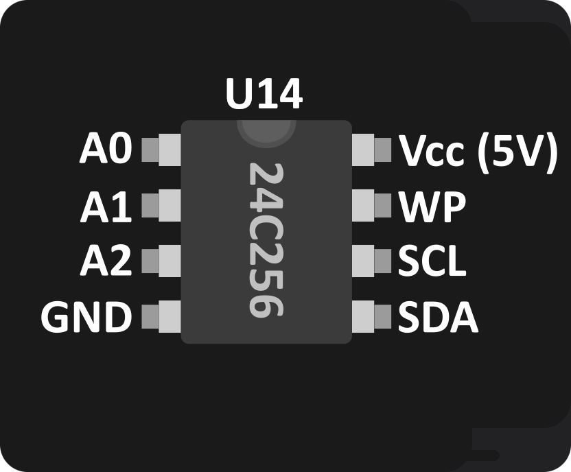
The signals are the following:
- $A_0$ to $A_2$: specifies the three lower bits of the 7-bit device address. The upper 4 bits are
1010. In the case of Zeal 8-bit Computer, these pins are connected to GND directly, so the 7-bit device address is0x50. Please note that $A_2$ is marked as $NC$ (Not connected) in the AT24C512 datasheet, but not in the 24LC256. In both cases, this doesn't change its address for us. - $V_{cc}$ and $Gnd$: main power supply (5V)
- $WP$: Write protect pin. In our case, it is connected to $Gnd$ so the EEPROM is never in write protect mode
- $SCL$ and $SDA$: I²C clock and data signals respectively, check the Inter-Integrated Circuit (I²C) section for more info.
14.3 Communicating with the EEPROM
Writing to the EEPROM
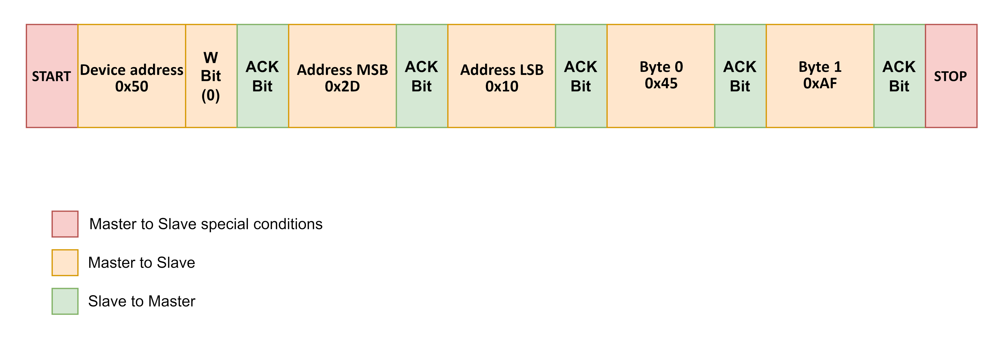
To write data to the EEPROM, it is required to perform an I²C write transaction with the following parameters:
0x50as the device address- 2 bytes for the address of the byte to write, MSB first
- $n$ bytes to be written starting at the address specified above
After sending a write command to the EEPROM, it will start processing it and do the actual write internally. During this process, it will stop responding to any other I²C requests. In other words, after writing, one way to know whether the EEPROM is ready again to accept new requests is to poll it with dummy read commands until it replies successfully.
For example, let's say the master wants to write the bytes 0x45 and 0xaf to address 0x2d10, the request will look like this:
Limitation
We can note that it is possible to write several bytes with a single transaction. However, keep in mind that the EEPROM is also paged, so it is not possible to write data that would cross the page boundary.
For example, the AT24C512 has 128-byte pages, the first page starts at 0x0000, the second one at 0x0080, the third one at 0x0100, etc...
As such, it is possible to perform a write of 128 bytes starting at 0x0000 but it is not possible to perform a write of 16 bytes starting at 0x0075, because the address of the last byte address would theoretically be 0x0085, which is a different page that the starting page.
In fact, in the latter case, the EEPROM will accept the write, but it will wrap the current write address, and so, will end up writing all the remaining bytes at the beginning of the page instead of "jumping" to the next page.
This limitation is documented in the official datasheet.
Reading from the EEPROM
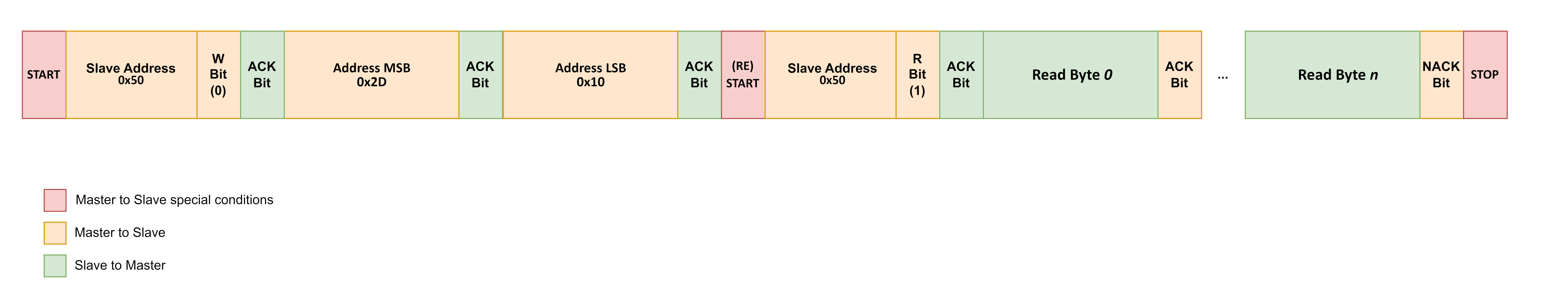
To perform a read of the EEPROM, two modes are available: Current Address mode and Random Read mode.
The Current Address mode is used when performing an I²C read operation. To determine the address of the byte to read, the EEPROM keeps an internal 16-bit buffer storing the current address. This address is incremented every time a byte is read in this mode.
The Random read mode is used when performing an I²C write-read operation. To determine the address of the byte to read, the master must first send (write) it and then start a read operation immediately after, without issuing a STOP condition. Similarly to the write mode, the 16-bit address must be sent MSB first. This mode will alter the internal current address buffer, so it can also be used to set its value.
Both modes support sequential reads, which lets the master retrieve the first, second, third, ..., $n^{th}$ bytes until a STOP is issued.
For example, let's say the master wants to read $n$ bytes starting at address 0x2d10, the following write-read operation can be used:
Note
It is important to note that in Current Address Read mode, the datasheet doesn't specify what the initial value is on power up, as such, it is safer to use that mode after using the Random read mode at least once.
14.4 Extending with more EEPROM
Thanks to the $A_0$, $A_1$, and $A_2$ pins, it is possible to interface up to 8 similar EEPROMs that have device addresses with 1010 in the upper bits.
As such, we can imagine an extension board that would connect to the user port and has three AT24C512 EEPROMs, making the total non-volatile I²C memory available 256KB.
These devices would need to see their $A_1$ and $A_0$ pins respectively connected as follows:
- GND, 5V (0, 1)
- 5V, GND (1, 0)
- 5V, 5V (1, 1)
As such, their respective device address would be 0x51, 0x52 and 0x53.