Inter-Integrated Circuit (I²C)
13.1 Overview
At the time of writing, some constraints that were chosen for this project led to a few choices of components for the motherboard. Indeed, integrated devices presenting a parallel interface while being in DIP format are rarer and rarer, newer devices are usually in SMD format and not even running out of 5V anymore.
An exception to that is I²C devices, such as EEPROMs, sensors or real-time clocks. These devices present a very small footprint, they take up a small space on the PCB, they can usually work with different voltages, including 5V and they use the same communication protocol: Inter-Integrated Circuit, or I²C, sometimes also called the two-wire interface.
The main advantage of this protocol is the number of lines it requires: two. The first one is SCL, for the clock, and the second one is SDA for the data. As it is a multi-master and multi-slave protocol, all the devices we want to communicate with will be connected to these two lines. Moreover, because there is a clock line, we can be as slow as we want without affecting the integrity of the transmitted data.
13.2 Hardware implementation
Similarly to the UART previously discussed, the I²C SDA and SCL lines originated from three I/Os from the Z80 PIO.
However, two of them, SDA OUT and SCL OUT, go through the 74LS07 integrated circuit that acts as an open-drain buffer.
Indeed, I²C protocol requires SDA and SCL lines to be in an open-drain configuration. This means that they can only be pulled low by the master or the devices, and a pull-up resistor must maintain them high when they are in a high-impedance state.
In the case of Zeal 8-bit Computer, the output signals of the 74LS07 are tied to Vcc through a 4.7kΩ resistors array, referenced RN3 on the PCB. This value of resistance is fairly typical and lets us reach 100KHz with faster transitions than when using the more classic 10kΩ.
Of course, the PIO should also be able to check the current status of the SDA line because it is a bi-directional line, so it is also routed to one of the I/Os.
Overall, the I²C bus on Zeal 8-bit Computer is organized as follows:

13.3 Protocol description
As said above, I²C is a multi-master and multi-device that relies on two lines: a clock line and a data line. For the sake of simplicity, in this part, we will only consider that we have a single master, which is Zeal 8-bit Computer in our case.
By default, when the bus is idle, both the clock line, SCL and the data line, SDA are held high. Again, this is done through a pull-up resistor.
The master initiates all the transfers, there is no way for devices to start an asynchronous transfer using I²C only, this means that the master has to poll the devices in case it is waiting for a particular event to happen. To communicate with a given device, the master has to know its address: each slave device has a 7-bit or 10-bit address, described in the datasheet. Here, we will only consider 7-bit addresses. They are always described in the device's datasheet.
Moreover, no matter if the transaction is a read or a write, the master also clocks the bus. In other words, the master toggles the SCL line. Connected devices are only allowed to change the data line (SDA) when the SCL line is low. As soon as the SCL line goes high, they are not allowed to alter the states of the lines.
A transfer is composed of:
- A start condition: the SDA line goes low when the SCL line is still high.
- The slave address: written by the master on the SDA line.
- The $read$/$\overline{write}$ bit: written by the master, tells the slave if the transaction is a read or a write.
- The slave ACK bit: if any device recognizes its address, it acknowledges it by pulling the SDA line low.
- $n$ data frames: each frame is 8-bit, in the case of a read, it is written by the slave, in the case of a write, it is written by the master. Each frame is followed by an ACK bit which is controlled by the master or the slave respectively.
- A stop condition: the SDA line goes high when the SCL line is high.
For the details related to the status of each line during a transfer, please refer to the official I²C specification.
📚 Going further
To have some asynchronous transfers initiated by the slave, some I²C devices may present some extra signals to let the master know that an event just happened and data are available to read. In fact, these extra signals can be an interrupt signal or a simple GPIO, that would tell the CPU (master) to initiate a transfer with that slave as it received an event.
Typical read transfer
The following diagram shows what a read transfer looks like in terms of data:
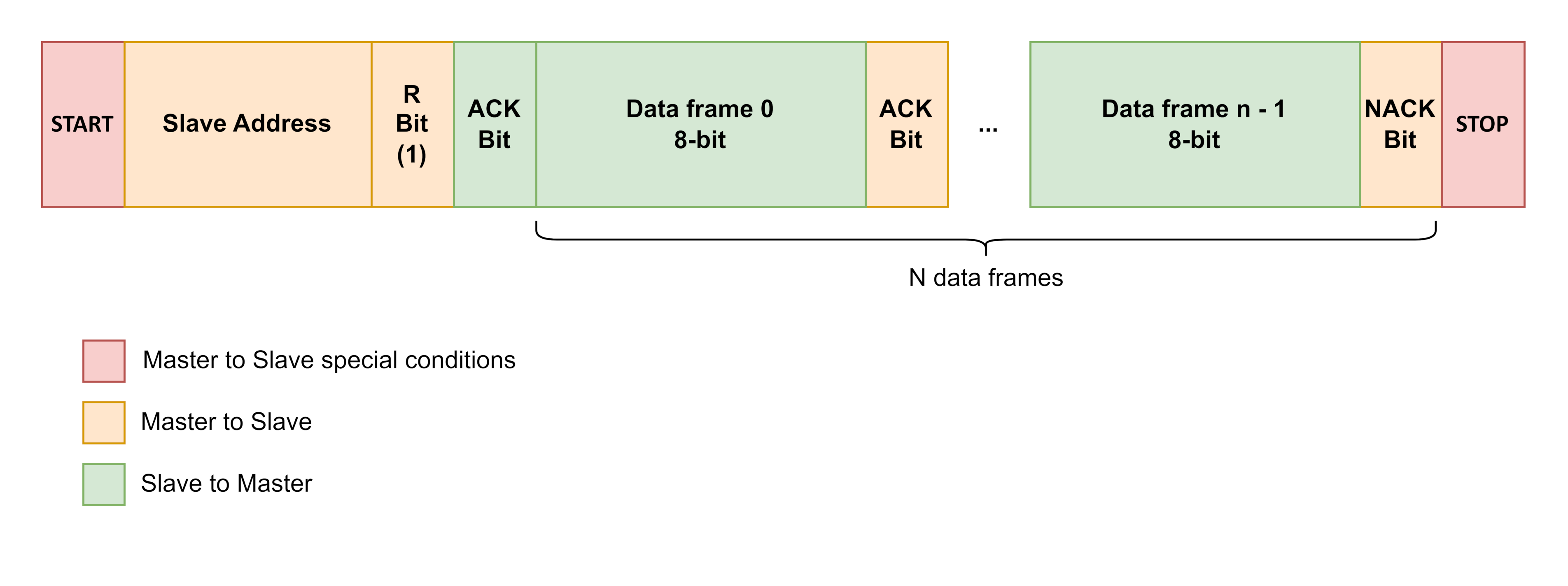
It is important to note that during a read transfer, after each byte, except the last one, received by the master, the SDA line is pulled low to mark an ACK bit. Indeed, the last byte received by the master must be followed by a NACK bit, which is represented by the SDA line being pulled high.
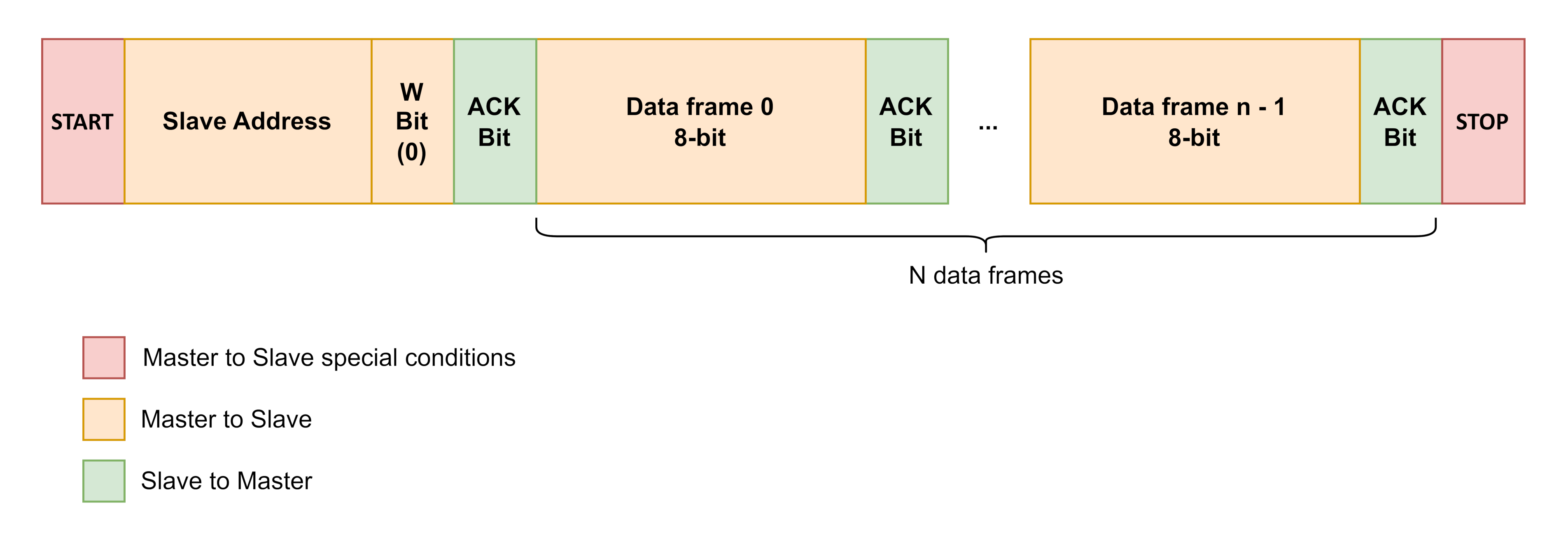
Typical write transfer
Performing a write transaction is very similar, except that the bit sent after the slave address is a 1 (SDA line pulled high) and the data frames are sent by the master to the slave. Of course, in that case, the ACK bits are sent from the slave:
The following diagram shows what a read transfer looks like in terms of data:
Typical write-read transfer
In most cases, a read transfer is not enough to specify the exact data that shall be read from the slave device. Indeed, devices usually have internal registers or indexed data.
For example, if the slave device is an EEPROM, the master will most likely want to specify from which address the data must be retrieved, else, it would need to read the whole EEPROM to get the data it wants.
The I²C protocol has a special transfer that lets a master first write data to a slave before receiving some data from a slave. This transaction is a write-read and looks like the following diagram:
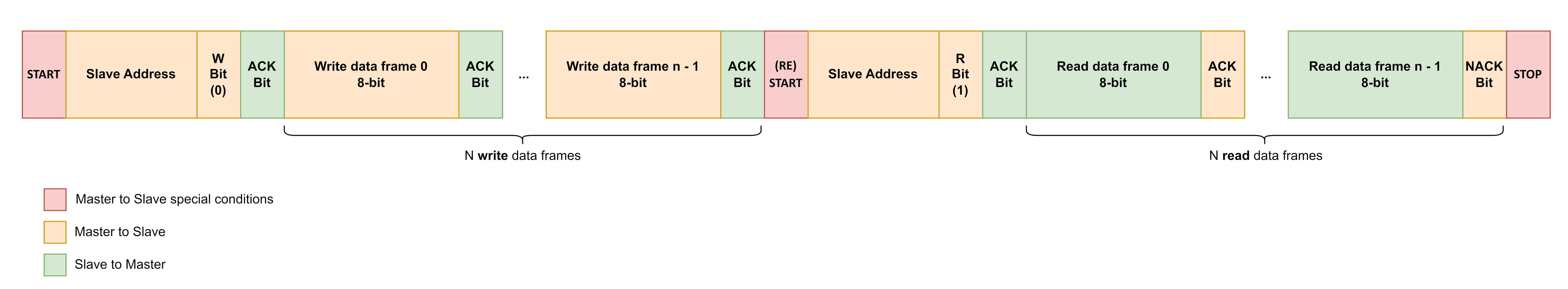
It is interesting to note that there is a restart condition before the second transfer, which is a read, and no stop condition in between.
The number of data frames to write first, before reading, is dependent on the device and shall be checked in its datasheet. It is usually either one or two bytes big. In the case of Zeal 8-bit Computer, the internal I²C devices only require a single byte to be written before the related data reading.
13.4 Limitation
Similarly to the UART, because the I²C lines are driven by the software, the clock speed is limited by the CPU speed. As such, with a 50% duty cycle, Zeal 8-bit Computer's I²C clock can reach the standardized 100KHz.
With more optimization and without a 50% duty cycle constraint, it is possible to reach a faster clock speed, around 120-130KHz, but this is not recommended.
Once again, an example of how to implement such a protocol can be found in Zeal 8-bit Bootloader source code.
13.5 Internal I²C connector
The I²C lines are available to the user from the user port. This lets anyone create external modules that can contain one or more I²C devices.
However, there is also an internal connector, referenced J5 on the PCB that presents these SCL and SDA lines. Its goal is mainly to be used in the future for internal purposes, for example inside a case, but at the moment it can still be freely used by users who need it.
This connector is a standard 5-pin XH2.54mm male connector with a lock. Any 2.54mm XH female connector can fit in. Its pinout is as follows:
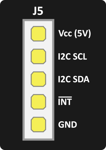
Which are:
- $Vcc$ and $GND$: 5V power supply and ground respectively
- $I^2C\ SCL$: open-drain I²C clock signal generated by the software. This signal is pull-up to 5V, make sure the device to connect to it is 5V-tolerant.
- $I^2C\ SDA$: open-drain I²C data signal generated by the software. This signal is pull-up to 5V, make sure the device to connect to it is 5V-tolerant.
- $\overline{INT}$: open-drain interrupt line connected to the Z80 CPU. This line is pulled low whenever a device wants to trigger an interrupt on the CPU. Make sure the device that generates the interrupt is compatible with the Z80 Mode 2 interrupt mode!