Memory Management Unit (MMU)
7.1 Overview
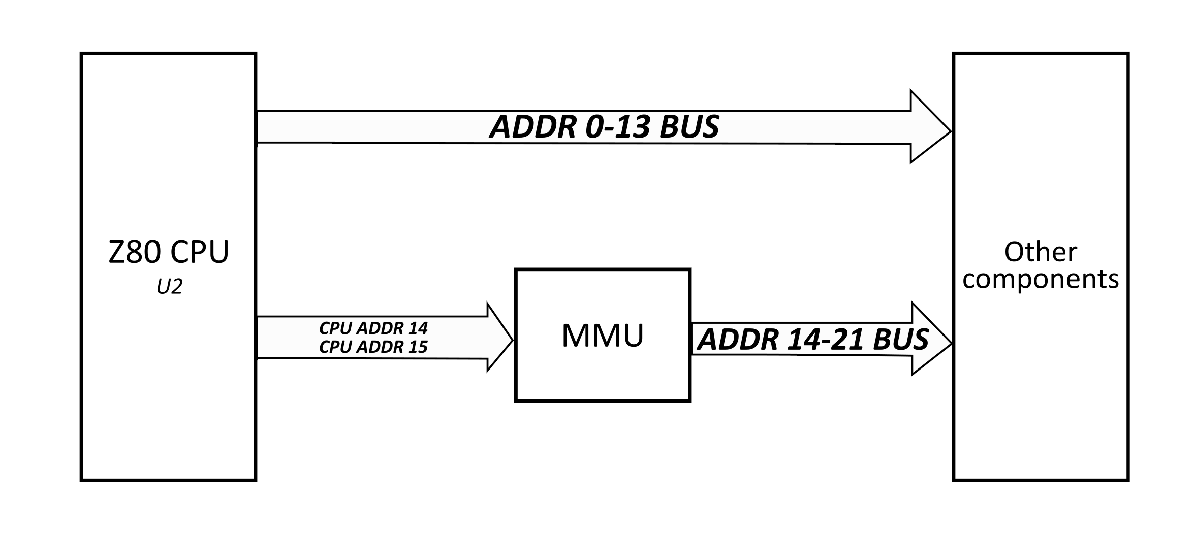
As explained in the previous section about the processor, the Z80 presents 16 address lines, in other words, it can handle addresses of 16-bit. This means that the maximum reachable address is 64KB, or 0xFFFF, in hexadecimal. This seems very low compared to modern computers which can address 32-bit or 64-bit addresses, but when the Z80 came out, it was more than enough as RAM and ROM were also very limited in size.
Regarding Zeal 8-bit Computer, 64KB is not enough. Indeed, the RAM itself is as big as 512KB, which already surpasses this limit. The solution to overcome this issue is to add a Memory Management Unit, or MMU, also known as Memory Mapper on some 8-bit computers. Its goal will be to give the CPU access to only a certain 64KB portion of the memory and hide the rest. Of course, the CPU will also be able to tell the MMU which portion of memory should be mapped and made accessible to it.
In our case, the part of the memory that is accessible by the CPU is called virtual memory, whereas the whole memory accessible through the MMU is called physical memory. The first one has a size of 64KB while the latter has a size of 4MB.
7.2 Hardware description
The Memory Management Unit is made out of three chips:
- Two 4-by-4 register files: 74HC670, referenced
U8andU9on the board - One octal buffer driver: 74HC541, referenced
U10
In our case, the register files are connected in parallel to store four 8-bit values. The first register file, referenced U8, manages the upper 4 bits, whereas the second one, U9, manages the lower 4 bits of each byte.
Each 8-bit value represents a virtual page and stores the highest address lines, or extended lines, of it. Thus, at any time, while the CPU is mastering the buses and performing a memory operation, the MMU must be read to get the physical memory address to read or write.
The pinout of the register files is as follows:
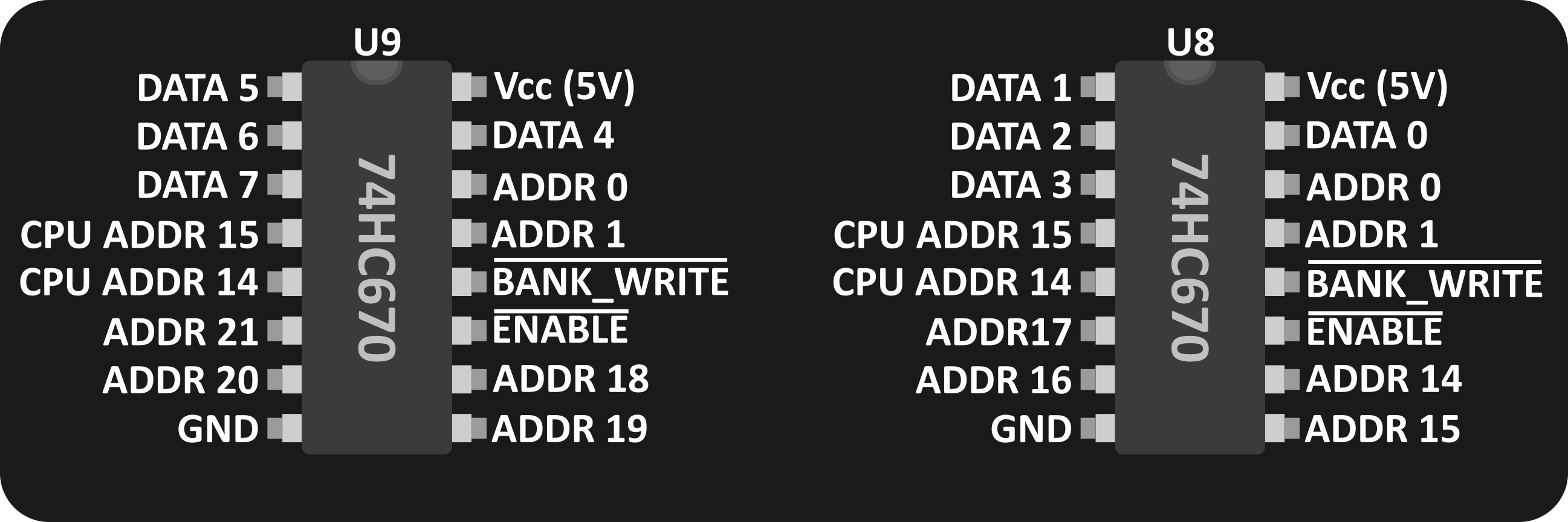
Where the signals are:
- $DATA\ 0$ to $DATA\ 7$: data bus shared between the CPU and all the other components.
- $ADDR\ 0$ and $ADDR\ 1$: address lines coming from the CPU. These lines, together, form a 2-bit value used to index the MMU page to write when $\overline{BANK\_WRITE}$ is active.
- $ADDR\ 14$ to $ADDR\ 21$: output of the MMU, these 8 lines represent the upper 8-bits of the physical address the CPU is currently trying to read or write. These lines are accessible through the extension port, the video card connector and all the components on the board.
- $CPU\ ADDR\ 14$ and $CPU\ ADDR\ 15$: input lines coming from the Z80 CPU. These lines, together, form a 2-bit value used to index the MMU page to read when $\overline{ENABLE}$ is active. The MMU is the only circuit that makes use of these two CPU lines, in the rest of this document, $ADDR 14$ and $ADDR 15$ refer to the output of the MMU.
- $\overline{BANK\_WRITE}$: write signal coming from the logic glue. When this signal is low, the page indexed by
[ADDR0, ADDR1]is written to the value present on lines $DATA\ 0$ to $DATA\ 7$. - $\overline{ENABLE}$: when low, the MMU outputs the current page value, indexed by
[ADDR0, ADDR1], on $DATA\ 0$ to $DATA\ 7$ lines. On Zeal 8-bit Computer, this line is only set to high when the Z80 CPU loses bus arbitration. Check Disabling the MMU section for more details.
These two register files are not enough to be able to read back the page configuration from the CPU, this is where the octal buffer driver comes in. When the CPU tries to read the MMU configuration, the buffer will redirect the MMU output to the DATA bus:
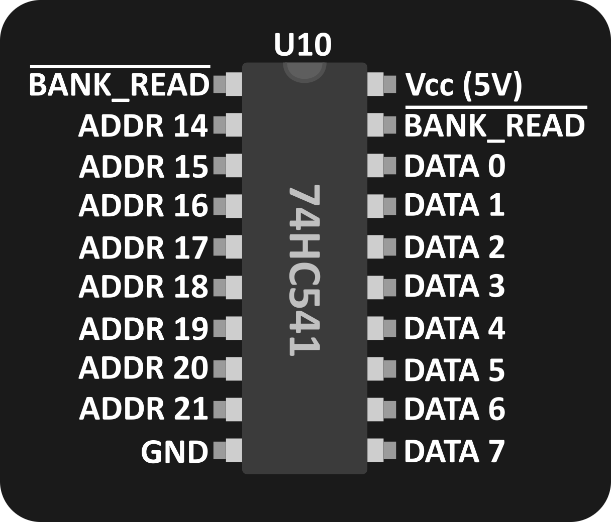
Where the signals are:
- $DATA\ 0$ to $DATA\ 7$: data bus shared between the CPU and all the other components.
- $ADDR\ 14$ and $ADDR\ 21$: output lines of the register files above.
- $\overline{BANK\_READ}$: line coming from the logic glue. Active when the CPU tries to read back the value of a page.
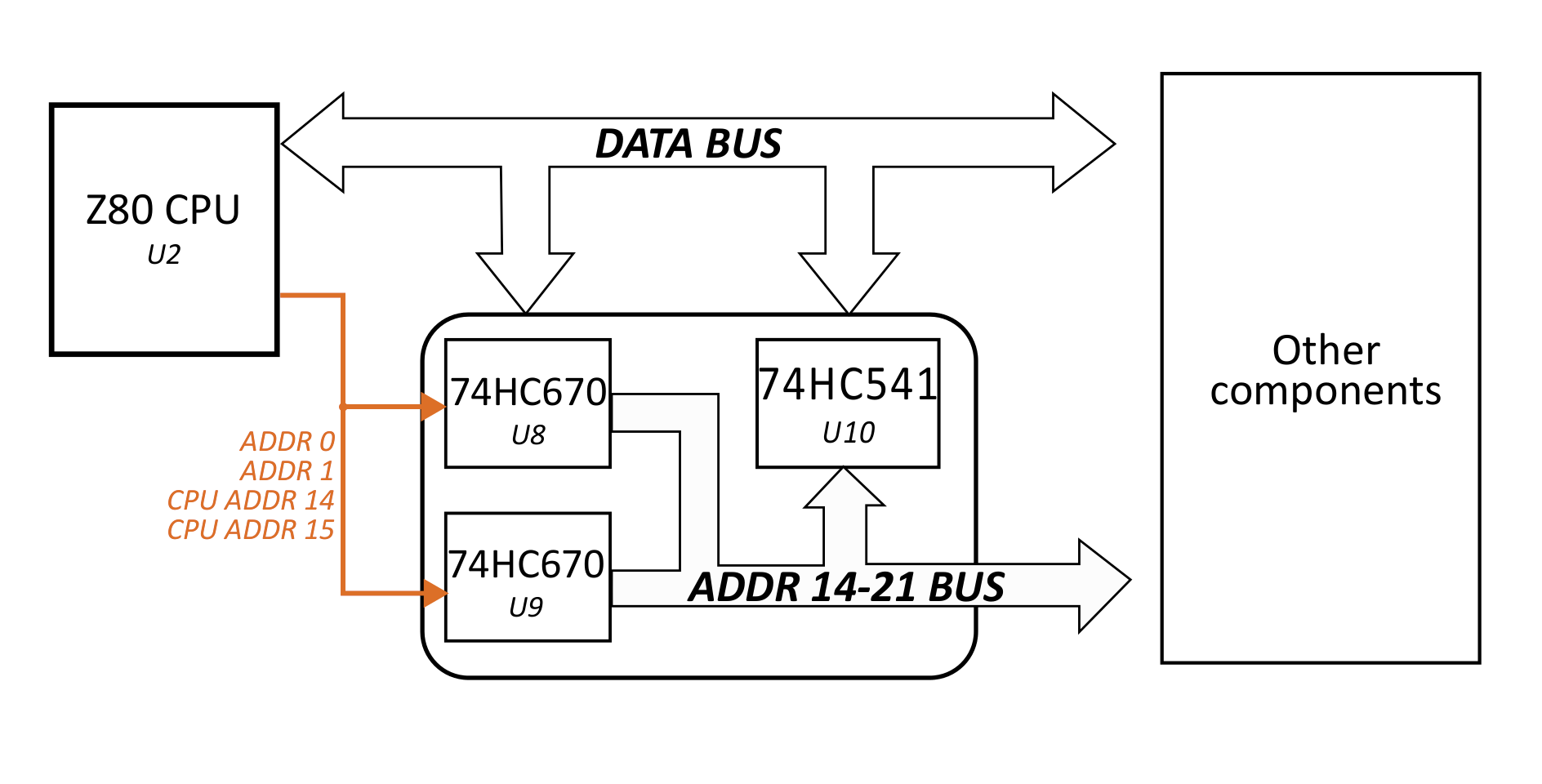
Overall, these components can be seen as interacting as follows:
Write MMU configuration
The MMU is also writeable, this is necessary to switch the part of the memory that the CPU wants to access. To do so, both register files write inputs are connected to an active low $\overline{MMU\_WRITE}$ signal, generated by the Logic Glue. This signal will be activated during an IO request when the given I/O address is comprised between 0xF0 and 0xFF.
The index of the page to write is formed by connecting CPU address lines ADDR 1, corresponding to bit 1, and ADDR 0, corresponding to bit 0, to both register files' Wa and Wb inputs respectively.
The address lines comprised between ranges ADDR 15...ADDR 8 and ADDR 3...ADDR 2 will be ignored. As such, writing to I/O address 0xF1, for example, will have the same effect as writing to I/O address 0xF9.
On reset, an MMU_WRITE signal is emitted, initializing the first page, of index 0, with the value 0x00. The CPU will therefore start executing the instruction located at physical address 0x000000 on boot up and resets.
Read MMU configuration
The I/O addresses given in the previous section are not enough to read back the configuration.
Indeed, because of the way the MMU read input pins are connected, reading back the configuration is slightly more complex than writing it. As explained in the section Virtual memory segmentation below, register files read input pins are connected to CPU address lines ADDR 15 and ADDR 14, as such, when reading back the configuration, these lines should also represent the index of the page to retrieve.
Even though the Z80 I/O bus is officially documented and used as an 8-bit bus, the address lines ADDR 15...ADDR 8 are still valid. Check the Z80 16-bit I/O requests table to see the value they take.
When a read MMU I/O request is detected, the value of the requested page is outputted on both register files data lines (Q0...Q4), and the octal buffer driver, referenced U10, is activated. Its role is to redirect these output lines to the CPU data lines. The CPU is then able to get the 8-bit value given by the register files.
For a practical example of how to read the MMU configuration, check the example section.
7.3 Virtual memory segmentation
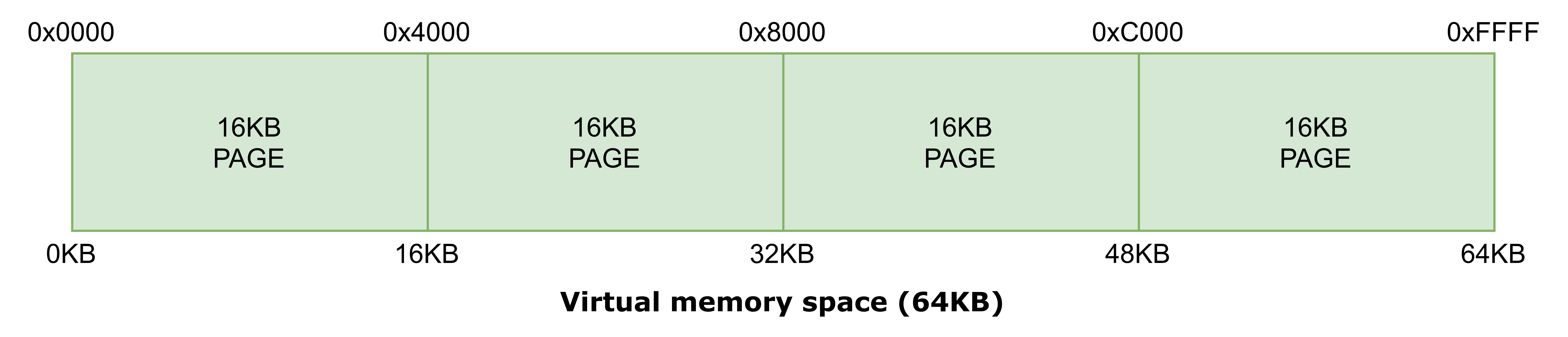
At runtime, to select which of the four 8-bit values to output, the highest two bits of the CPU address lines, ADDR 14 and ADDR 15 are extracted and interpreted as a 2-bit value. Thus, the pair [ADDR 15, ADDR 14] can take any value between 0 and 3. This is the read entry for both register files.
The remaining 14-bit address is the offset within the virtual memory page. Therefore, a single virtual page has a size of 16KB. We can see [ADDR 15, ADDR 14] as the page index to get data from or write data to.
After this page index is given to the register files, they output an 8-bit value, representing the highest bits of the physical memory address. We will call this range EXT_ADDR21...EXT_ADDR14. By concatenating the output of the register files and the CPU remaining address lines ADDR13...ADDR0, we get a 22-bit physical address.
By programming the content stored in the register files, we can control which 16KB window will be seen by the CPU at a given virtual page.
Symmetrically, by reading the configuration of a virtual page, we can know which physical address is currently being mapped to a virtual address.
7.4 Disabling the MMU
It is important to note that when the $\overline{BUSACK}$ signal is low, the MMU is disabled. In other words, if any other device than the CPU is mastering the buses, it will need to manage all the 22-bit of the address manually. For example, a DMA chip would not be able to interact with or use the MMU, even for reading its configuration. Nevertheless, this also means that such a DMA-capable device would also be able to alter any part of the physical memory, even if it is not mapped on the virtual address space.
7.5 MMU examples
In the following examples, the following macros will be used:
DEFC MMU_PAGE0    0xF0
DEFC MMU_PAGE1    0xF1
DEFC MMU_PAGE2    0xF2
DEFC MMU_PAGE3    0xF3
They define the I/O address of each page. The following macros define the virtual addresses where each virtual page start:
DEFC VIRT_ADDR_PAGE0    0x0000
DEFC VIRT_ADDR_PAGE1    0x4000
DEFC VIRT_ADDR_PAGE2    0x8000
DEFC VIRT_ADDR_PAGE3    0xC000
Write configuration
The following example configures the MMU to map a given physical address:
; Map the first 16KB of RAM to the second virtual page. In other words, map physical address 0x80000 to virtual address 0x4000
ld a, 0x80000 >> 14
out (MMU_PAGE1), a
; We can do the same thing using c an another register
ld b, 0x80000 >> 14
ld c, MMU_PAGE1
out (c), b
Read configuration
The following example reads the MMU configuration for the third page:
; Put in A upper 2 bits the page index to read, 0b10 in our case (index 2)
ld a, 0x80 ; = 0b1000_0000 in binary
in a, (MMU_PAGE2) ; In practice, we can use any MMU_PAGEn, but for easier understanding and reading, it is advised to use the actual page to read.
; A register now contains the upper 8 bits of the 22-bit physical address mapped to virtual address 0x8000
It is also possible to perform this operation using c register, but in this case, the page index must be put in b register's upper two bits:
ld b, 0x80
ld c, MMU_PAGE2
; We can then read the 8-bit value of the third page n any register:
in a, (c)
; or E
in e, (c)
; or even B! But in that case, this would destruct the previously written upper bits
in b, (c)
Backup and restore configuration
In some cases, it may be necessary to store the current configuration of a virtual page to modify it freely and restore it before returning.
Let's say for example that a print function needs to map a VRAM area first before actually printing on the screen the characters. Then it needs to restore the original configuration and return it to the caller:
; We suppose that:
;   - SP, Stack Pointer, points to the last page (0xC000-0xFFFF)
;   - PC, Program Counter, is in the first page (0x0000-0x3FFF)
;   - HL contains the string to print
print_screen:
    ; Get the configuration of the second page
    ld a, 0x80 ; 0b1000_0000 in binary
    in a, (MMU_PAGE1)
    ; Store the given value on the stack
    push af
    ; Map the VRAM in the second page
    ld a, VRAM_PHYS_ADDR >> 14 ; we suppose this macro exists
    out (MMU_PAGE1), a
    ; Do what we have to do with VRAM
    [...]
    ; Restore the original configuration
    pop af
    out (MMU_PAGE1), a
    ret