PS/2 Keyboard
16.1 Overview
As we saw earlier, UART is a bi-directional communication protocol, it can be used to receive and send data. It can be used to receive characters from another computer and be interpreted as if they were directly typed for our 8-bit computer.
However, this raises a few questions. UART is mainly used to send ASCII characters (or raw bytes for data), no there is no standard way to send special keyboard keys like Ctrl, Alt or function keys. Moreover, we would always need another computer, or at least a monitor to receive inputs.
Installing a standard PS/2 keyboard interface can solve both issues.
16.2 PS/2 protocol
The PS/2 protocol is based on two bi-directional open-drain lines: a clock line and a data line. Both lines are pulled up when idling, as such, the data line is ready and stable when the clock signal is on a falling edge.
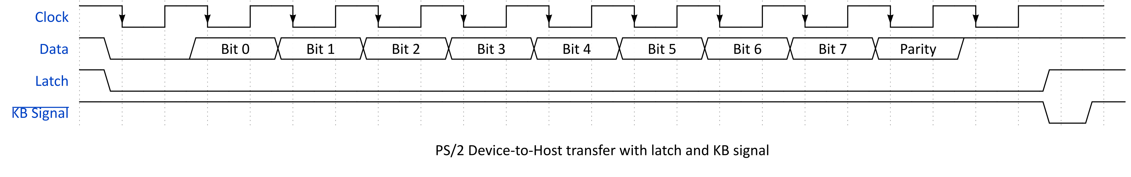
Whenever a key is pressed on the keyboard, the latter will start toggling the clock line while outputting a start bit, 8-bit corresponding to the key code, a stop bit and a parity bit. Therefore, each transfer is composed of 11 bits. The keyboard will prepare the bit to send when the clock is high and keep it stable while the clock is low. The following diagram shows how a byte is sent to the host computer:

When a key is released on the keyboard, an additional transaction will be sent to the computer by the keyboard. This transaction is composed of a break code (0xF0) followed by the code of the released key. In case the case where the pressed key has a 2-byte scan code starting with 0xE0, the break code 0xF0 is placed right after 0xE0.
The code for each key depends on the keyboard scan set number. Most of the PS/2 keyboards use scan code set 2, let's use it as an example in the rest of the section. The following table shows the scan codes for each key:
| Key name | Key pressed code | Key released code | Key name | Key pressed code | Key released code |
|---|---|---|---|---|---|
| ESC | 76 | F0 76 | K | 42 | F0 42 |
| F1 | 05 | F0 05 | L | 4B | F0 4B |
| F2 | 06 | F0 06 | ; | 4C | F0 4C |
| F3 | 04 | F0 04 | ' | 52 | F0 52 |
| F4 | 0C | F0 0C | Enter | 5A | F0 5A |
| F5 | 03 | F0 03 | Shift (Left) | 12 | F0 12 |
| F6 | 0B | F0 0B | Z | 1A | F0 1A |
| F7 | 83 | F0 83 | X | 22 | F0 22 |
| F8 | 0A | F0 0A | C | 21 | F0 21 |
| F9 | 01 | F0 01 | V | 2A | F0 2A |
| F10 | 09 | F0 09 | B | 32 | F0 32 |
| F11 | 78 | F0 78 | N | 31 | F0 31 |
| F12 | 07 | F0 07 | M | 3A | F0 3A |
| Prt Scr | E0 12 E0 7C | E0 F0 7C E0 F0 12 | , | 41 | F0 41 |
| Scroll Lock | 7E | F0 7E | . | 49 | F0 49 |
| Pause | E1 14 77 E1 F0 14 E0 77 | None | / | 4A | F0 4A |
| ` | 0E | F0 0E | Shift (right) | 59 | F0 59 |
| 1 | 16 | F0 16 | Ctrl (left) | 14 | F0 14 |
| 2 | 1E | F0 1E | Windows (left) | E0 1F | E0 F0 1F |
| 3 | 26 | F0 26 | Alt (left) | 11 | F0 11 |
| 4 | 25 | F0 25 | Space | 29 | F0 29 |
| 5 | 2E | F0 2E | Alt (right) | E0 11 | E0 F0 11 |
| 6 | 36 | F0 36 | Windows (right) | E0 27 | E0 F0 27 |
| 7 | 3D | F0 3D | Menu | E0 2F | E0 F0 2F |
| 8 | 3E | F0 3E | Ctrl (right) | E0 14 | E0 F0 14 |
| 9 | 46 | F0 46 | Insert | E0 70 | E0 F0 70 |
| 0 | 45 | F0 45 | Home | E0 6C | E0 F0 6C |
| - | 4E | F0 4E | Page Up | E0 7D | E0 F0 7D |
| = | 55 | F0 55 | Delete | E0 71 | E0 F0 71 |
| Backspace | 66 | F0 66 | End | E0 69 | E0 F0 69 |
| Tab | 0D | F0 0D | Page Down | E0 7A | E0 F0 7A |
| Q | 15 | F0 15 | Up Arrow | E0 75 | E0 F0 75 |
| W | 1D | F0 1D | Left Arrow | E0 6B | E0 F0 6B |
| E | 24 | F0 24 | Down Arrow | E0 72 | E0 F0 72 |
| R | 2D | F0 2D | Right Arrow | E0 74 | E0 F0 74 |
| T | 2C | F0 2C | Num Lock | 77 | F0 77 |
| Y | 35 | F0 35 | / (numpad) | E0 4A | E0 F0 4A |
| U | 3C | F0 3C | * (numpad) | 7C | F0 7C |
| I | 43 | F0 43 | - (numpad) | 7B | F0 7B |
| O | 44 | F0 44 | 7 (numpad) | 6C | F0 6C |
| P | 4D | F0 4D | 8 (numpad) | 75 | F0 75 |
| [ | 54 | F0 54 | 9 (numpad) | 7D | F0 7D |
| ] | 5B | F0 5B | + (numpad) | 79 | F0 79 |
| \ | 5D | F0 5D | 4 (numpad) | 6B | F0 6B |
| CapsLock | 58 | F0 58 | 5 (numpad) | 73 | F0 73 |
| A | 1C | F0 1C | 6 (numpad) | 74 | F0 74 |
| S | 1B | F0 1B | 1 (numpad) | 69 | F0 69 |
| D | 23 | F0 23 | 2 (numpad) | 72 | F0 72 |
| F | 2B | F0 2B | 3 (numpad) | 7A | F0 7A |
| G | 34 | F0 34 | 0 (numpad) | 70 | F0 70 |
| H | 33 | F0 33 | . (numpad) | 71 | F0 71 |
| J | 3B | F0 3B | Enter (numpad) | E0 5A | E0 F0 5A |
16.3 Hardware implementation
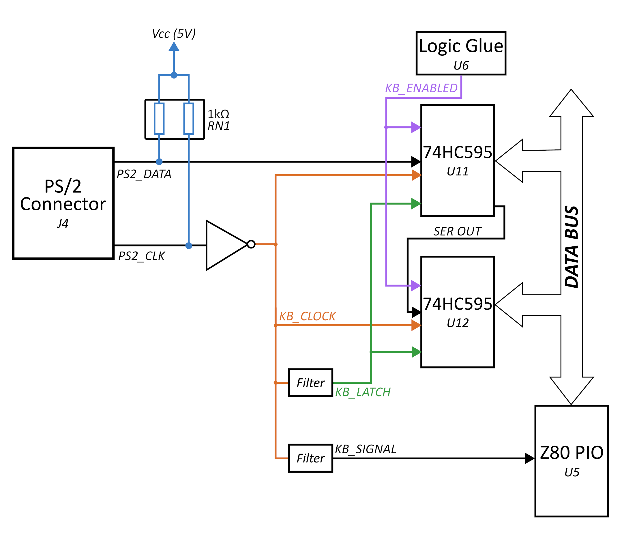
Zeal 8-bit Computer presents a mini DIN-6 connector, referenced J4 on the PCB, meant to accommodate a standard PS/2 keyboard. Its data and clock lines are pulled up thanks to the resistor network reference RN1, marked at 1kΩ.
For Zeal 8-bit Computer, the choice was made to perform the decoding on the hardware rather than software and to only do it with 7400 logic chips. While using a microcontroller for the decoding process would have been feasible and even more straightforward, it would have compromised the authentic retro feel of the board. Moreover, opting for logic chips instead of microcontrollers ensures a more transparent board, as the latter can be seen as black boxes that operate with a level of inherent complexity.
The first part for decoding is made out of two 74HC595 serial-to-parallel shift registers, referenced U11 and U12 on the PCB.
They are responsible for storing the incoming byte from the keyboard when a key is pressed or released. Even though they are capable of storing 16 bits together, only 8 bits end up being used and wired to the CPU data bus. Indeed, using all 16 bits would have required more components and more glue logic.
Moreover, these registers can only store up to 8-bit at a time, they don't have any FIFO or RAM underneath. This means that if the Z80 CPU doesn't read the incoming byte fast enough, it will be lost as soon as another keyboard event occurs.
Shift registers pinout
The pinout for these shift registers is as followed:
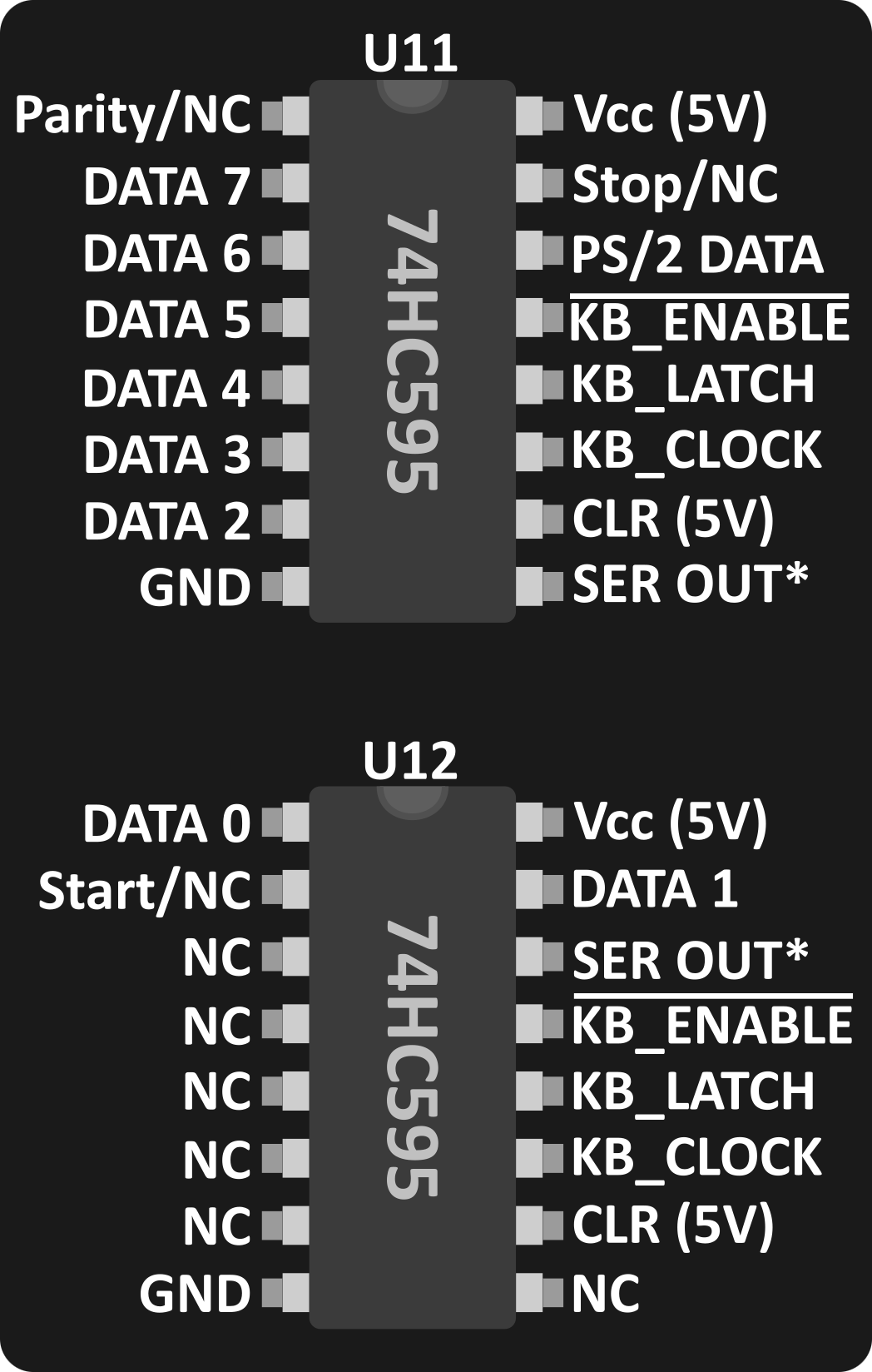
The signals are:
- $DATA\ 0$ to $DATA\ 7$: 8-bit of data coming from PS/2 keyboard. These are directly connected to Z80 CPU data bus. As such, the 8 bits received will only be outputted on the bus when $\overline{KB\_ENABLED}$ is active (low).
- $SER\ OUT$: these two pins are connected together. When more than 8 bits have been shifted in the first shift register
U11, the highest bit is shifted out of the component to welcome a new one. That bit is outputted through this pin. As such, this highest bit becomes the second shift register,U12lowest bit. - $Parity$, $Stop$, $Start$: when $\overline{KB\_ENABLED}$ is active (low), these pins contain the parity bit, 1 and 0 respectively. These are not connected to anything on Zeal 8-bit Computer.
- $PS/2\ DATA$: Data line coming from the PS/2 keyboard.
- $KB\_CLOCK$: inverted PS/2 clock signal. Since the 74HC595 requires an active high clock to shift the incoming data, and the PS/2 clock line is active low, an inverter, referenced
U7, is used to invert the latter signal and connect it to the shift registers. - $KB\_LATCH$: signal triggering a latch of the shifted bits inside the internal buffer. This signal is active high, so the latch occurs on rising edges. Check the complementary signals generation subsection below for more information.
- $\overline{KB\_ENABLED}$: active low signal coming from the logic glue. This line is low when the CPU is trying to read the bits currently stored inside the shift registers.
- $\overline{CLR}$: clears data stored internally when low. Hardwired to 5V in our case, do not attempt to connect it to any other signal.
- $5V$ and $Gnd$: power supply.
- $NC$: Not connected.
Complementary signals generation
The first signal that needs to be generated for the components above is $KB\_LATCH$. Indeed, even if the bits have been shifted in the registers, it is not enough to be able to output them on the data bus. It is required to latch them to another internal buffer, which itself outputs its content on $DATA\ 0$...$DATA\ 7$ lines when $\overline{KB\_ENABLED}$ becomes active.
On Zeal 8-bit Computer, this $KB\_LATCH$ is generated thanks to a resistor-capacitor circuit (RC circuit) and an inverter which makes the signal low until the last bit was transferred. The following diagram shows what the latch signal looks like during a transfer:

As soon as the latch signal goes high (rising edge), the shift registers will latch the shifted bits inside their internal 8-bit buffers.
There is one more signal that is not directly related to the shift registers but is still generated by the PS/2 decoder circuit: $\overline{KB\ Signal}$, an active low signal connected to the Z80 PIO System port, that notifies the latter when a new byte has been shifted in from the keyboard and is now ready to be read.
To generate this signal, a differentiator is used, also composed of a capacitor and a resistor, and an inverter, also referenced U7.
Block Diagram
The following block diagram summarizes the interaction between the PS/2 keyboard, the decoder and the PIO:
Passive components
To ease maintenance of the PS/2 decoder circuits, the following table sums up the required parts that are used, with their references on the PCB and their respective values:
| Part | Reference | Value | Description |
|---|---|---|---|
| Diode | D2 | 1N4148 | Used for $KB\_LATCH$ |
| Diode | D3 | 1N4148 | Used for $\overline{KB\ Signal}$ |
| Capacitor | C17 | 100nF | Used for $KB\_LATCH$ |
| Capacitor | C18 | 100nF | Used for $\overline{KB\ Signal}$ |
| Resistor | R8 | 2kΩ | Used for $KB\_LATCH$ |
| Resistor | R9 | 470Ω | Used for $\overline{KB\ Signal}$ |
| Resistor | R10 | 20kΩ | Used for $\overline{KB\ Signal}$ |
16.4 Timings
As said previously, when a key is pressed or released, the keyboard will toggle the clock line and transfer the actual key code scan to the host. The PS/2 protocol specifies that the clock frequency is between 10KHz and 16.7KHz, which means one clock period is between 60µs and 100µs.
Since the $KB\_LATCH$ signal is generated from the clock signal itself, it will be affected by the frequency too. However, it will always see its rising edge after the last clock period, so it will never last shorter than a transaction.
Similarly, $\overline{KB\_SIGNAL}$ will always see its falling edge occurring when $KB\_LATCH$ goes high. It will stay low for around 18µs, regardless of the PS/2 clock frequency.
The following diagram sums up the timing for the keyboard decoder, keep in mind this is not 100% accurate as the timings depend on the capacitors and resistors on the board:

Where:
- $p$ is the period of the PS/2 clock signal, $60µs ≤ p ≤ 100µs$
- $e$ is the delay between the first falling edge fo the clock and the falling edge of the latch signal, $e ≃5µs$
- $d$ is the delay between the last clock rising edge and the latch signal rising edge, in practice it is around $104µs$
- $s$ is the duration of the $\overline{KB\_SIGNAL}$, $s ≃18µs$
Note: the timings have been measured on a 13.15KHz PS/2 keyboard.
16.5 Limitations
Bi-directional communication
PS/2 protocol states that clock and data lines are in open-drain configuration, which is also the case on Zeal 8-bit Computer. The main purpose of this is to be able to have host-to-device communications. Indeed, the host should be able to send commands to the keyboard to tell it to reset, resend the last byte, turn on/off the LEDs, etc...
However, because of the way the protocol is decoded (with logic chips only) on Zeal 8-bit Computer and also for space reasons, the communication is unidirectional and can only be done from the keyboard to the PIO/CPU. As such, it is not possible to tell the keyboard to power on some LEDs like the "Num Lock" or "Caps Lock" ones.
Keyboard interrupt source
When a byte is sent from the keyboard, it triggers an interrupt thanks to $\overline{KB\_SIGNAL}$ signal. However, that signal doesn't clear itself when the CPU reads the incoming byte. As such, if another interrupt source from the PIO system port comes in, the PIO won't trigger a second interrupt, even if the CPU has already finished and returned from the Interrupt Service Routine, or ISR.

The first interrupt occurs because the $\overline{KB\_SIGNAL}$ signal goes active (low), the CPU reads the status of the PIO System port, which is 0x7F, handles the keyboard interrupt and returns from the ISR with reti instruction.
Afterward, the V-blank signal goes active, but as the $\overline{KB\_SIGNAL}$ is still active, the PIO won't trigger a second interrupt. As such, the V-blank interrupt will be lost and never handled.
📝 Note
The assumption that the PIO System port is configured in bitcontrol/OR/Active-low mode was made.
Software workaround
The simplest way to overcome this issue would be to enable a single interrupt source at a time so that when an interrupt occurs, it is obvious which device triggered it.
The other solution would be to make the ISR long enough so that when the CPU returns from it, the keyboard signal is inactive (high). This also implies that the ISR will have to check if any other interrupt source went active in the meanwhile.
The keyboard signal lasts around 18µs, which corresponds to 180 T-States on Zeal 8-bit Computer.
Let's say both the keyboard and the V-blank interrupts are enabled, the ISR would look like the following:
    ; Interrupt handler invoked by the CPU in mode 2
pio_isr:
    ; Use the CPU alternate registers for the ISR
    ex af, af'
    exx

    ; Read the state of the PIO system port to determine which line is low.
    in a, (0xD1)

    ; Check for KB_SIGNAL (Bit 7)
    bit 7, a
    call z, keyboard_isr

    ; If we entered keyboard_isr routine, A contains the latest state of PIO System port
    ; Check for V-blank (Bit 6)
    bit 6, a
    call z, vblank_isr

    ; Return from the interrupt
    exx
    ex af, af'
    ei
    reti

keyboard_isr:
    ; Read byte received by the keyboard
    in a, (0xE0)
    ; Handle the byte...
    [...]

    ; Wait for the signal to go high
_keyboard_isr_low:
    in a, (0xD1)
    bit 7, a
    ret nz
    jr _keyboard_isr_low

vblank_isr:
    ; Handle V-Blank ISR, do not alter A
    ; Clear the V-blank interrupt!
    ret
Hardware workaround
In hardware, to overcome this problem, it is possible to add a diode (1N4148 type) between diode's D3 cathode and shift register U12's pin 13 ($\overline{KB\_ENABLED}$).
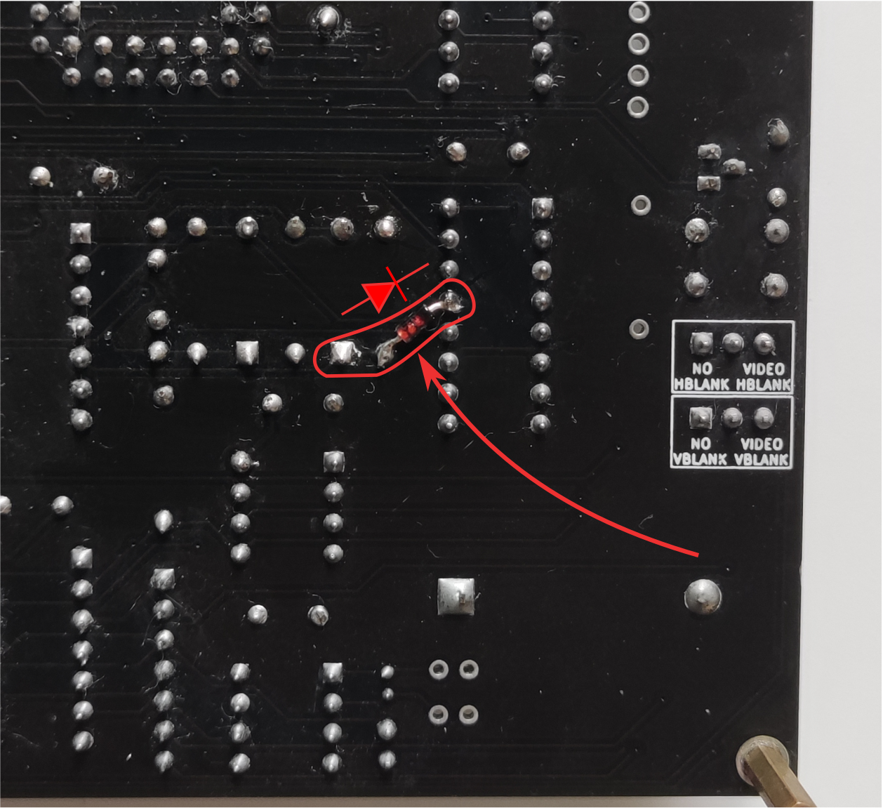
Adding this diode will let the $\overline{KB\_SIGNAL}$ clear itself automatically as soon as the CPU tries to read from the byte that was just received.
Therefore, the ISR does not need to wait for the keyboard signal to go high anymore:
    ; Interrupt handler invoked by the CPU in mode 2
pio_isr:
    ; Use the CPU alternate registers for the ISR
    ex af, af'
    exx

    ; Read the state of the PIO system port to determine which line is low.
    in a, (0xD1)
    ; Only keep the bits we are interested in
    and 0xc0

pio_isr_check:
    ; Check for KB_SIGNAL (Bit 7)
    bit 7, a
    call z, keyboard_isr

    ; Check for V-blank (Bit 6)
    bit 6, a
    call z, vblank_isr

    ; Check if any signal changed since the beginning
    ld b, a
    in a, (0xD1)
    and 0xc0
    cp b
    ; If any bit changed, handle the new signals
    jr nz, pio_isr_check

    ; Return from the interrupt
    exx
    ex af, af'
    ei
    reti

keyboard_isr:
    ; Read byte received by the keyboard, this will
    ; automatically clear the signal
    in a, (0xE0)
    ; Handle the byte...
    [...]
    ret

vblank_isr:
    ; Handle V-Blank ISR, do not alter A
    ; Clear the V-blank interrupt!
    ret